9DBV0641
9DBV0641 is 6-Output 1.8V PCIe Zero-Delay/Fanout Clock Buffer manufactured by Renesas.
Description
The 9DBV0641 is a member of Renesas’ 1.8V Very-Low-Power (VLP) PCIe family. It has integrated output terminations providing Zo = 100 for direct connection to 100 transmission lines. The device has 6 output enables for clock management and 3 selectable SMBus addresses.
Remended Application
1.8V PCIe Gen1- 5 Zero Delay/Fanout Buffer (ZDB/FOB)
Output Features
- Six 1- 200 MHz Low-Power (LP) HCSL DIF pairs with
Zo = 100
Key Specifications
- DIF cycle-to-cycle jitter < 50ps
- DIF output-to-output skew < 50ps
- PCIe Gen5 CC additive phase jitter < 40fs RMS
- 12k Hz- 20MHz additive phase jitter = 156fs RMS at
156.25MHz (typical)
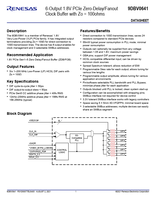
Block Diagram v OE(5:0)#
Features
/Benefits
- Direct connection to 100 transmission lines; saves 24 resistors pared to standard PCIe devices
- 55m W typical power consumption in PLL mode; minimal power consumption
- Outputs can optionally be supplied from any voltage between 1.05 and 1.8V; maximum power savings
- OE# pins; support DIF power management
- HCSL patible differential input; can be driven by mon clock sources
- Spread Spectrum tolerant; allows reduction of EMI
- Programmable Slew rate for each output; allows tuning for various line lengths
- Programmable output amplitude; allows tuning for various application environments
- Pin/software selectable PLL bandwidth and PLL Bypass; minimize phase jitter for each application
- Outputs blocked until PLL is locked; clean system start-up
- Configuration can be acplished with strapping pins;
SMBus interface not required for device control
- 3.3V tolerant SMBus interface works with legacy controllers
- Space saving 5 × 5mm 40-VFQFPN; minimal board space
- 3 selectable SMBus addresses; multiple devices can easily share an SMBus segment
CLK_IN CLK_IN# v SADR ^v HIBW_BYPM_LOBW# ^CKPWRGD_PD# SDATA_3.3 SCLK_3.3
SSpatible
CONTROL LOGIC
DIF5 DIF4 DIF3 DIF2 DIF1 DIF0
9DBV0641 R31DS0077EU0400 AUGUST 2, 2021
©2021 Renesas Electronics...