9FGL0441 Description
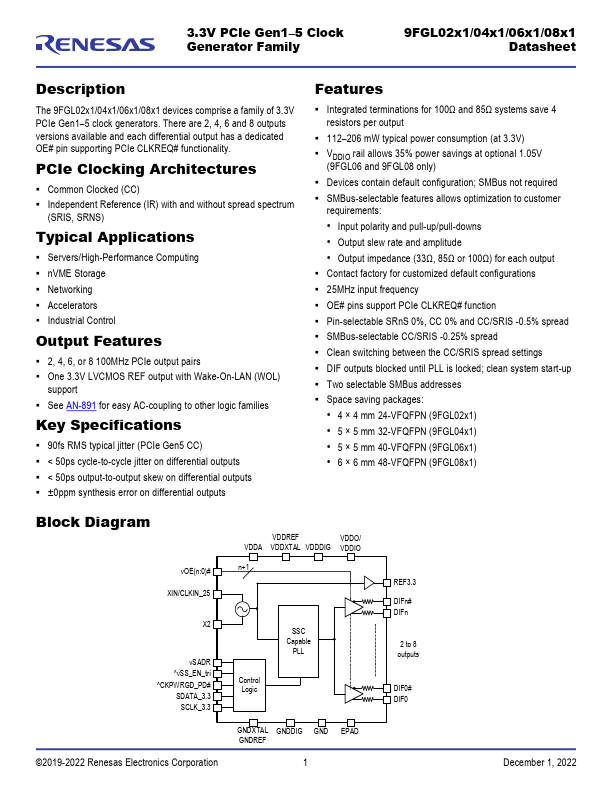
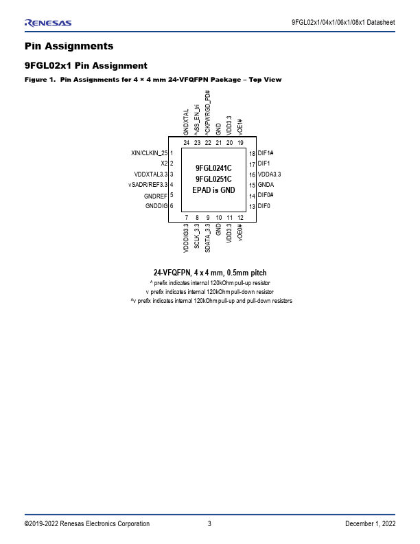
The 9FGL02x1/04x1/06x1/08x1 devices prise a family of 3.3V PCIe Gen1 5 clock generators. There are 2, 4, 6 and 8 outputs versions available and each differential output has a dedicated OE# pin supporting PCIe CLKREQ# functionality. PCIe Clocking Architectures mon Clocked (CC) Independent Reference (IR) with and without spread spectrum (SRIS, SRNS) Typical Applications Servers/High-Performance puting nVME Storage...
9FGL0441 Key Features
- 2, 4, 6, or 8 100MHz PCIe output pairs
- One 3.3V LVCMOS REF output with Wake-On-LAN (WOL)
- See AN-891 for easy AC-coupling to other logic families
- 90fs RMS typical jitter (PCIe Gen5 CC)
- < 50ps cycle-to-cycle jitter on differential outputs
- < 50ps output-to-output skew on differential outputs
- ±0ppm synthesis error on differential outputs
- Integrated terminations for 100Ω and 85Ω systems save 4 resistors per output
- 112-206 mW typical power consumption (at 3.3V)
- VDDIO rail allows 35% power savings at optional 1.05V