9FGV1006C Overview
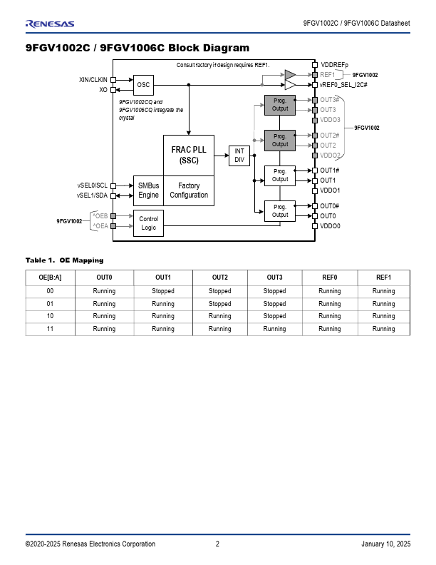
The 9FGV1002C / 9FGV1006C are members of the Renesas’ PhiClock™ programmable clock generator family. These devices are optimized for low phase noise spread-spectrum applications such as PCIe® Express. Four user-defined configurations may be selected via two hardware select pins or two I2C bits, allowing easy software selection of the desired configuration.
9FGV1006C Key Features
- 2 or 4 programmable output pairs plus 1 or 2 LVCMOS REF outputs
- 1MHz-325MHz LVDS or LP-HCSL outputs
- 1MHz-200MHz LVCMOS outputs
- 1.8V, 2.5V or 3.3V core power supplies
- Individual 1.8V, 2.5V or 3.3V VDDO for each output pair
- 40°C to +85°C operation
- standard product
- 40°C to +105°C operation
- 9FGV1002C automotive product
- Direct connection to HCSL, LVDS and LVCMOS inputs