9ZXL1251
9ZXL1251 is 12-Output DB1200ZL Derivative manufactured by Renesas.
Description
The 9ZXL1251 meets the demanding requirements of the Intel DB1200ZL specification, including the critical low-drift requirements of Intel CPUs. It is pin patible to the 9ZXL1231 and integrates 24 termination resistors, saving 41mm2 board area.
Applications
Buffer for Romley, Grantley and Purley Servers, solid state storage and PCIe
Output Features
- 12 LP-HCSL Output Pairs w/integrated terminations
(Zo = 85Ω)
Key Specifications
- Cycle-to-cycle jitter < 50ps
- Output-to-output skew < 50ps
- Input-to-output delay variation < 50ps
- PCIe Gen3 phase jitter < 1.0ps RMS
- Phase jitter: QPI/UPI > = 9.6GB/s < 0.2ps rms
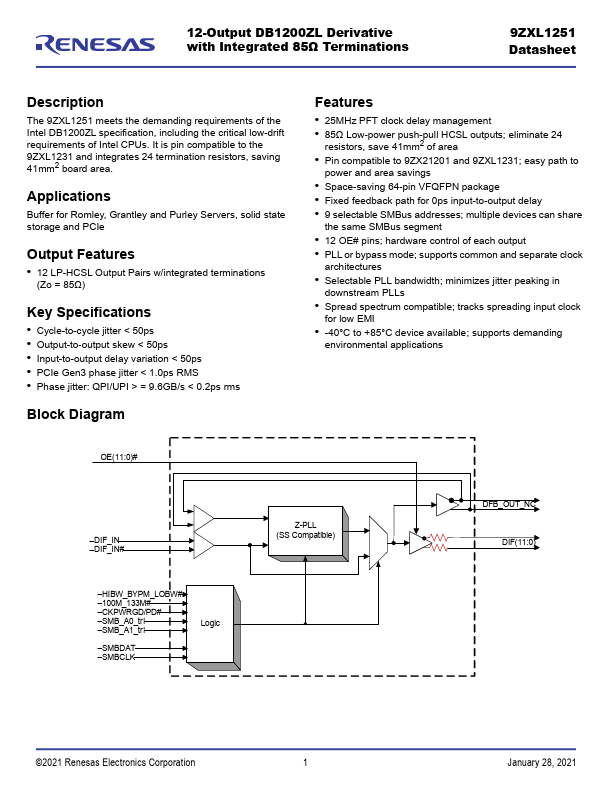
Block Diagram
Features
- 25MHz PFT clock delay management
- 85Ω Low-power push-pull HCSL outputs; eliminate 24 resistors, save 41mm2 of area
- Pin patible to 9ZX21201 and 9ZXL1231; easy path to power and area savings
- Space-saving 64-pin VFQFPN package
- Fixed feedback path for 0ps input-to-output delay
- 9 selectable SMBus addresses; multiple devices can share the same SMBus segment
- 12 OE# pins; hardware control of each output
- PLL or bypass mode; supports mon and separate clock architectures
- Selectable PLL bandwidth; minimizes jitter peaking in downstream PLLs
- Spread spectrum patible; tracks spreading input clock for low EMI
- -40°C to +85°C device available; supports demanding environmental applications
OE(11:0)#
DIF_IN DIF_IN#
HIBW_BYPM_LOBW# 100M_133M# CKPWRGD/PD# SMB_A0_tri SMB_A1_tri SMBDAT SMBCLK
Logic
Z-PLL (SS patible)
DFB_OUT_NC DIF(11:0)
©2021 Renesas Electronics Corporation
January 28, 2021
Pin Configuration
9ZXL1251 Datasheet
DIF_11# DIF_11 v OE11# v OE10# DIF_10# DIF_10 GND VDD VDDIO DIF_9# DIF_9 v OE9# v OE8# DIF_8# DIF_8 VDDIO
64 63 62 61 60 59 58 57 56 55 54 53 52 51 50 49
VDDA...