EL5624A
EL5624A is 6-Channel Buffer manufactured by Renesas.
features a slew rate of 15V/µs. The output current is rated at 30m A continuous, 140m A peak.
The V amplifier is rated for 260m A peak output current and also features higher slew rate (70V/µs) and bandwidth (35MHz) for use in error cancellation circuits.
The EL5624A is available in the 20-pin HTSSOP package and is specified for operation over the -40°C to +85°C temperature range.
Ordering Information
PART NUMBER (See Note)
PACKAGE (Pb-Free)
TAPE & REEL PKG. DWG. #
EL5624AIREZ (See Note)
20-Pin HTSSOP (Pb-free)
- MDP0048
EL5624AIREZ-T7 20-Pin HTSSOP
(See Note)
(Pb-free)
7"
MDP0048
EL5624AIREZ-T13 20-Pin HTSSOP
(See Note)
(Pb-free)
13"
MDP0048
NOTE: Intersil Pb-free products employ special Pb-free material sets; molding pounds/die attach materials and 100% matte tin plate termination finish, which are Ro HS pliant and patible with both Sn Pb and Pb-free soldering operations. Intersil Pb-free products are MSL classified at Pb-free peak reflow temperatures that meet or exceed the Pb-free requirements of IPC/JEDEC J STD-020.
FN7506 Rev 0.00 February 14, 2005
Features
- 6 x gamma buffers
- Single high power V amplifier
- 260m A peak V output current
- Low power
- just 8.5m A
- Pb-free available (Ro HS pliant)
Applications
- TFT-LCD displays
- Flat panel monitors
- Notebook displays
- LCD-TVs
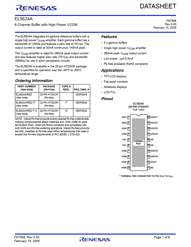
Pinout
EL5624A (20-PIN HTSSOP)
TOP VIEW
VIN1 1
20 VOUT1
VIN2...