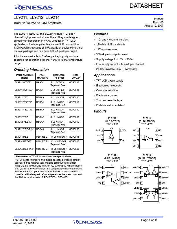
Description
CONDITIONS
MIN MAX (Note 2) TYP (Note 2) UNIT
INPUT CHARACTERISTICS
VOS TCVOS IB RIN CIN VREG CMIR
Input Offset Voltage Average Offset Voltage Drift Input Bias Current Input Impedance Input Capacitance Load Regulation Common Mode Input Range
VCM = 6V (Note 1) VCM = 6V
VCOM = 6V, -100mA < IL < 100mA
-6 -1 +2 mV
10 µV/C
-1.4 -0.4 µA
1 G
1.35 pF
-20 +20 mV
-0.5
+12.5
V
CMRR
Common Mode Rejection Ratio
AVOL
Open Loop Gain
OUTPUT CHARACTERISTICS
For VIN from -0.5 to +12.5V
75
Features
- a -3dB bandwidth of 130MHz with slew rates of 115V/µs. Each device comes in a thermal package and can drive 300mA peak per output. All units are available in Pb-free packaging only and are specified for operation over the -40°C to +85°C temperature range. Ordering Information
PART NUMBER
PART
(Note).