ICS9173B Key Features
- Phase-detector/VCO circuit block
- Ideal for genlock system
- Reference clock range 12 kHz to 1 MHz for full output
- On-chip loop filter
- Single 5 V power supply
- Low power CMOS technology
- 8-pin SOIC package
ICS9173B is VIDEO GENLOCK PLL manufactured by Renesas.
| Manufacturer | Part Number | Description |
|---|---|---|
| ICS9173-01 | Video Genlock PLL |
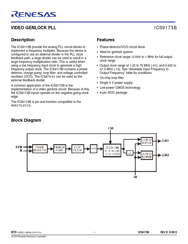
The ICS9173B provide the analog PLL circuit blocks to implement a frequency multiplier. Because the device is configured to use an external divider in the PLL clock feedback path, a large divider can be used to result in a large frequency multiplication ratio. This is useful when using a low frequency input clock to generate a high frequency output clock.