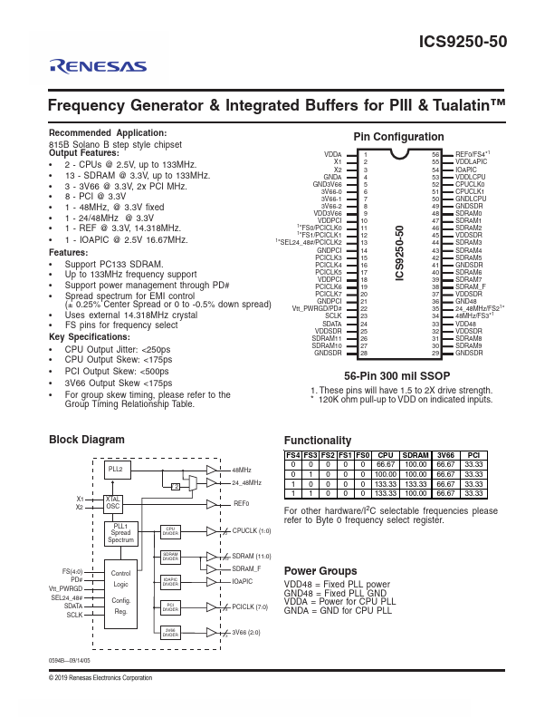
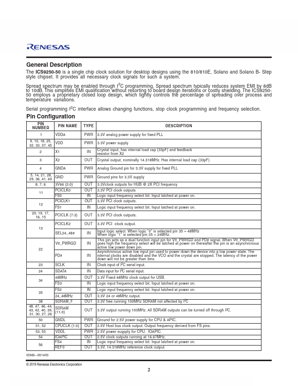
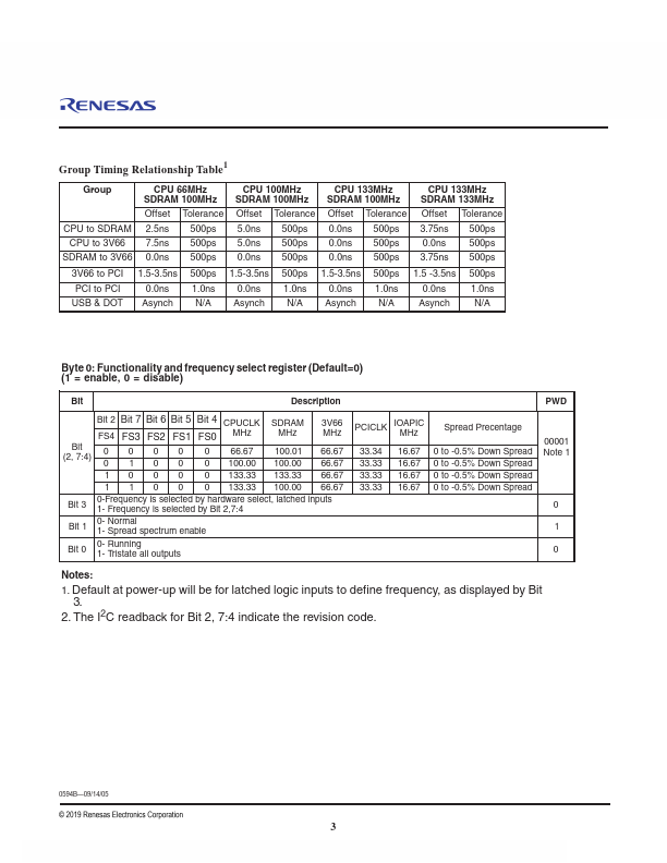
ICS9250-50
General Description
The ICS9250-50 is a single chip clock solution for desktop designs using the 810/810E, Solano and Solano B- Step
style chipset. It provides all necessary clock signals for such a system.
Spread spectrum may be enabled through I2C programming. Spread spectrum typically reduces system EMI by 8dB
to 10dB. This simplifies EMI qualification without resorting to board design iterations or costly shielding. The ICS9250-
50 employs a proprietary closed loop design, which tightly controls the percentage of spreading over process and
temperature variations.
Serial programming I2C interface allows changing functions, stop clock programming and frequency selection.
Pin Configuration
PIN
NUMBER
PIN NAME TYPE
DESCRIPTION
1
VDDA
PWR 3.3V analog power supply for fixed PLL
9, 10, 18, 25,
32, 33, 37, 45
VDD
2
X1
3
X2
PWR 3.3V power supply
IN
Crystal input, has internal load cap (33pF) and feedback
resistor from X2
OUT Crystal output, nominally 14.318MHz. Has internal load cap (33pF)
4
GNDA
5, 14, 21, 28,
29, 36, 41, 49
GND
8, 7, 6
3V66 (2:0)
11
PCICLK0
FS0
PCICLK1
12
FS1
20, 19, 17,
16, 15
PCICLK (7:3)
PCICLK2
13
SEL24_48#
Vtt_PWRGD
22
PD#
23
SCLK
24
SDATA
48MHz
34
FS3
FS2
35
24_48MHz
38
SDRAM_F
48, 47, 46, 44,
43, 42, 40, 39,
31, 30, 27, 26
SDRAM
(11:0)
50
GNDL
51, 52
CPUCLK (1:0)
53, 55
54
56
VDDL
IOAPIC
FS4
REF0
PWR Analog Ground pin for 3.3V supply for fixed PLL
PWR Ground pins for 3.3V supply
OUT
OUT
IN
OUT
IN
3.3Vclock outputs for HUB @ 2X PCI frequency
3.3V PCI clock outputs
Logic input frequency select bit. Input latched at power on.
3.3V PCI clock outputs.
Logic input frequency select bit. Input latched at power on.
OUT 3.3V PCI clock outputs.
OUT 3.3V PCI clock output.
IN
IN
IN
IN
IN
OUT
IN
IN
OUT
OUT
Input logic select. When logic "0" is selected pin 35 = 48MHz
When logic "1" is selected pin 35 = 24MHz.
This pin acts as a dual function input pin for Vtt_PWRGD and PD# signal. When Vtt_PWRGD
goes high the frequency select will be latched at power on thereafter the pin is an asynchronous
active low power down pin.
Asynchronous active low input pin used to power down the device into a low power state. The
internal clocks are disabled and the VCO and the crystal are stopped. The latency of the power
down will not be greater than 3ms.
Clock input of I2C serial input.
Data input for I2C serial input.
3.3V Fixed 48MHz clock output for USB.
Logic input frequency select bit. Input latched at power on.
3.3V 24 or 48MHz output.
3.3V free running 100MHz SDRAM not affected by I2C
OUT 3.3V output running 100MHz. All SDRAM outputs can be turned off through I2C.
PWR Ground for 2.5V power supply for CPU & APIC.
OUT 2.5V Host bus clock output. Output frequency derived from FS pins.
PWR
OUT
IN
OUT
2.5V power suypply for CPU, IOAPIC.
2.5V clock outputs running at 16.67MHz.
Logic input frequency select bit. Input latched at power on.
3.3V, 14.318MHz reference clock output.
0594B—09/14/05
2