Datasheet4U Logo Datasheet4U.com

ICS9DBL411A Datasheet - Renesas

Four Output Differential Fanout Buffer

ICS9DBL411A Features

* 4 - low power differential output pairs

* Individual OE# control of each output pair Key Specifications:

* Output cycle-cycle jitter < 25ps additive

* Output to output skew: < 50ps Features/Benefits:

* Low power differential fanout buffer for PCIExpress an

ICS9DBL411A General Description

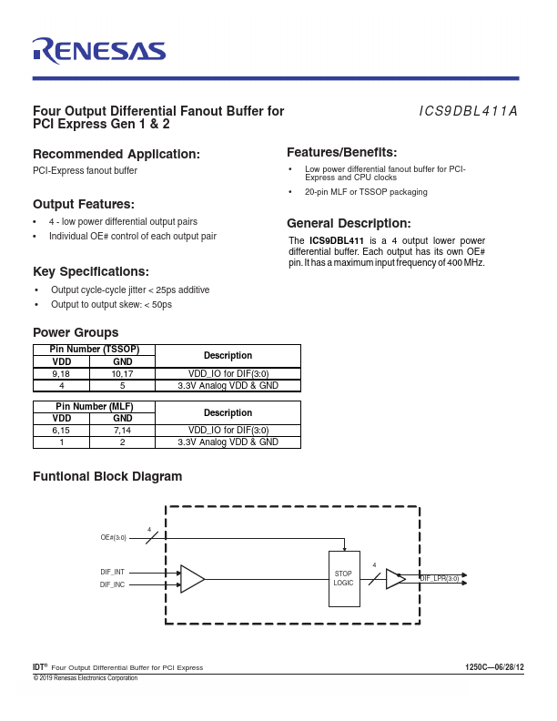
The ICS9DBL411 is a 4 output lower power differential buffer. Each output has its own OE# pin. It has a maximum input frequency of 400 MHz. Power Groups Pin Number (TSSOP) VDD GND 9,18 10,17 45 Pin Number (MLF) VDD GND 6,15 7,14 12 Description VDD_IO for DIF(3:0) 3.3V Analog VDD & GND D.

ICS9DBL411A Datasheet (189.86 KB)

Preview of ICS9DBL411A PDF

Datasheet Details

Part number:

ICS9DBL411A

Manufacturer:

Renesas ↗

File Size:

189.86 KB

Description:

Four output differential fanout buffer.
DATASHEET Four Output Differential Fanout Buffer for PCI Express Gen 1 & 2 ICS9DBL411A Recommended Application: PCI-Express fanout buffer Output Fe.

📁 Related Datasheet

ICS9DBL411 Four Output Differential Fanout Buffer (IDT)

ICS9DB102 Two Output Differential Buffer (IDT)

ICS9DB102 2 Output PCI Express Buffer (Integrated Circuit Systems)

ICS9DB102 Two Output Differential Buffer (Renesas)

ICS9DB104 Four Output Differential Buffer (Integrated Circuit Systems)

ICS9DB104 Four Output Differential Buffer (Renesas)

ICS9DB106 6 Output PCI Express Buffer (Integrated Circuit Systems)

ICS9DB108 Eight Output Differential Buffer (Integrated Circuit Systems)

ICS9DB108 Eight Output Differential Buffer (Renesas)

ICS9DB202 Two 0.7V current mode differential HCSL output pairs (Integrated Circuit Systems)

TAGS

ICS9DBL411A Four Output Differential Fanout Buffer Renesas

Image Gallery

ICS9DBL411A Datasheet Preview Page 2 ICS9DBL411A Datasheet Preview Page 3

ICS9DBL411A Distributor