IDT72V201
IDT72V201 is 3.3 VOLT CMOS SyncFIFO manufactured by Renesas.
FEATURES
:
- 256 x 9-bit organization IDT72V201
- 512 x 9-bit organization IDT72V211
- 1,024 x 9-bit organization IDT72V221
- 2,048 x 9-bit organization IDT72V231
- 4,096 x 9-bit organization IDT72V241
- 8,192 x 9-bit organization IDT72V251
- 10 ns read/write cycle time
- 5V input tolerant
- Read and Write clocks can be independent
- Dual-Ported zero fall-through time architecture
- Empty and Full Flags signal FIFO status
- Programmable Almost-Empty and Almost-Full flags can be set to any depth
- Programmable Almost-Empty and Almost-Full flags default to
Empty+7, and Full-7, respectively
- Output Enable puts output data bus in high-impedance state
- Advanced submicron CMOS technology
- Available in 32-pin plastic leaded chip carrier (PLCC) and 32-pin plastic Thin Quad Flat Pack (TQFP)
- Industrial temperature range (- 40°C to +85°C) is available
- Green parts available, see ordering information
DESCRIPTION
:
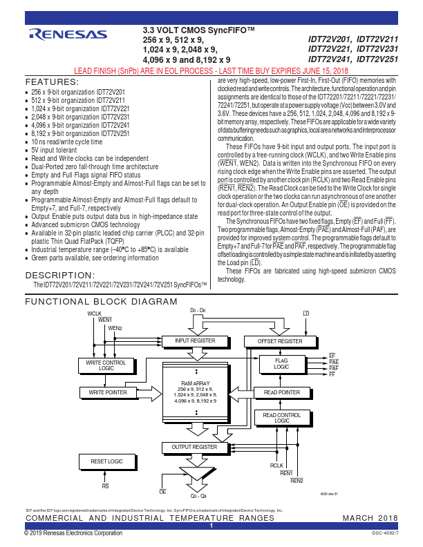
The IDT72V201/72V211/72V221/72V231/72V241/72V251 Sync FIFOs™ are very high-speed, low-power First-In, First-Out (FIFO) memories with clocked read and write controls. The architecture, functional operation and pin assignments are identical to those of the IDT72201/72211/72221/72231/ 72241/72251, but operate at a power supply voltage (Vcc) between 3.0V and 3.6V. These devices have a 256, 512, 1,024, 2,048, 4,096 and 8,192 x 9bit memory array, respectively. These FIFOs are applicable for a wide variety of data buffering needs such as graphics, local area networks and interprocessor munication.
These FIFOs have 9-bit input and output ports. The input port is controlled by a free-running clock (WCLK), and two Write Enable pins (WEN1, WEN2). Data is written into the Synchronous FIFO on every rising clock edge when the Write Enable pins are asserted. The output port is controlled by another clock pin (RCLK) and two Read Enable pins (REN1, REN2). The Read Clock can be tied to the Write Clock for single clock operation or the two clocks can run asynchronous of one another...