IDT72V3676
IDT72V3676 is CMOS TRIPLE BUS SyncFIFO manufactured by Renesas.
- Part of the IDT72V3656 comparator family.
- Part of the IDT72V3656 comparator family.
FEATURES
- Serial or parallel programming of partial flags
- Memory storage capacity: IDT72V3656
- 2,048 x 36 x 2
- Big- or Little-Endian format for word and byte bus sizes
- Loopback mode on Port A
IDT72V3666
- 4,096 x 36 x 2
- Retransmit Capability
- 8,192 x 36 x 2
- Master Reset clears data and configures FIFO, Partial Reset
- Clock frequencies up to 100 MHz (6.5ns access time)
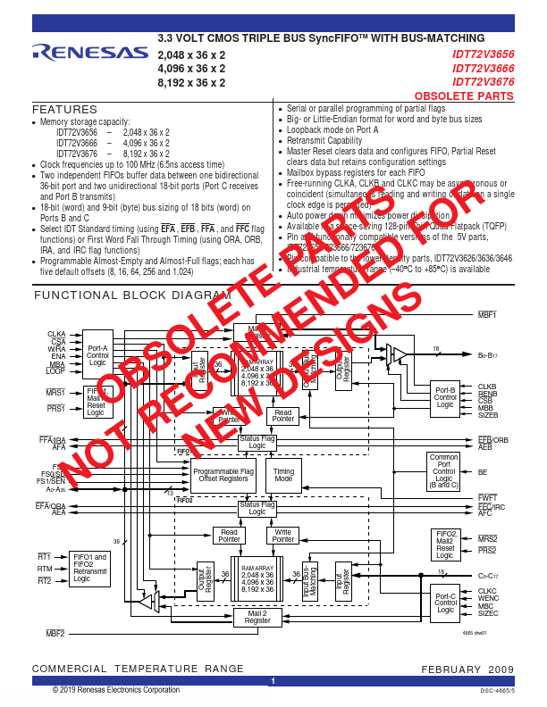
- Two independent FIFOs buffer data between one bidirectional
36-bit port and two unidirectional 18-bit ports (Port C receives and Port B transmits)
- 18-bit (word) and 9-bit (byte) bus sizing of 18 bits (word) on
S R Ports B and C T O
- Select IDT Standard timing (using EFA , EFB , FFA , and FFC flag functions) or First Word Fall Through Timing (using ORA, ORB,
R F IRA, and IRC flag functions) A
- Programmable Almost-Empty and Almost-Full flags; each has P D five default offsets (8, 16, 64, 256 and 1,024) clears data but retains configuration settings
- Mailbox bypass registers for each FIFO
- Free-running CLKA, CLKB and CLKC may be asynchronous or coincident (simultaneous reading and writing of data on a single clock edge is permitted)
- Auto power down minimizes power dissipation
- Available in a space-saving 128-pin Thin Quad Flatpack (TQFP)
- Pin and functionally patible versions of the 5V parts, IDT723656/723666/723676
- Pin patible to the lower density parts, IDT72V3626/3636/3646
- Industrial temperature range (- 40°C to +85°C) is available
E DE FUNCTIONAL BLOCK DIAGRAM
Input Register Output Bus Matching Output Register
ET EN NS CLKA L CSA O M IG W/RA
ENA MBA
S M S LOOP B O E MRS1 O C D PRS1 RE W FFA/IRA E AFA T N FS2 O FS0/SD
FS1/SEN
N A0-A35
Port-A Control Logic
FIFO1, Mail1 Reset Logic
Mail 1 Register
RAM ARRAY
2,048 x...