Datasheet4U Logo Datasheet4U.com

KAD5514P - 14-Bit ADC

General Description

.

.

2.

10 2.1 Absolute Maximum Ratings

Key Features

  • Programmable gain, offset, and skew control.
  • 950MHz analog input bandwidth.
  • 60fs clock jitter.
  • Over-range indicator.
  • Selectable clock divider: ÷1, ÷2, or ÷4.
  • Clock phase selection.
  • Nap and sleep modes.
  • Two’s complement, gray code or binary data format.
  • DDR LVDS-compatible or LVCMOS outputs.
  • Programmable built-in test patterns.
  • Single-supply 1.8V operation.
  • Pb-free (RoHS compliant) Key Spe.

📥 Download Datasheet

Full PDF Text Transcription (Reference)

The following content is an automatically extracted verbatim text from the original manufacturer datasheet and is provided for reference purposes only.

View original datasheet text
Datasheet KAD5514P 14-Bit, 250/210/170/125MSPS ADC The KAD5514P (KAD5514P-12, KAD5514P-17, KAD5514P-21, KAD5514P-25) is a family of low-power, high performance 14-bit, analog-to-digital converters. 
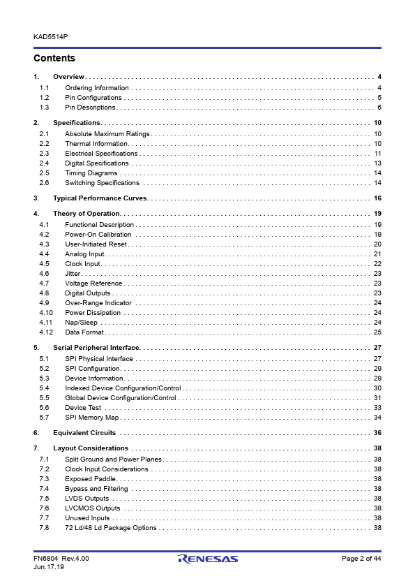
The family is designed with the proprietary FemtoCharge™ technology on a standard CMOS process, and supports sampling rates of up to 250MSPS. The KAD5514P is part of a pin-compatible portfolio of 10, 12, and 14-bit ADCs with sample rates ranging from 125MSPS to 500MSPS. A Serial Peripheral Interface (SPI) port allows for extensive configurability and fine control of various parameters such as gain and offset. Digital output data is presented in selectable LVDS or CMOS formats. The KAD5514P is available in 72 Ld and 48 Ld QFN packages with an exposed paddle. The devices operate from a 1.