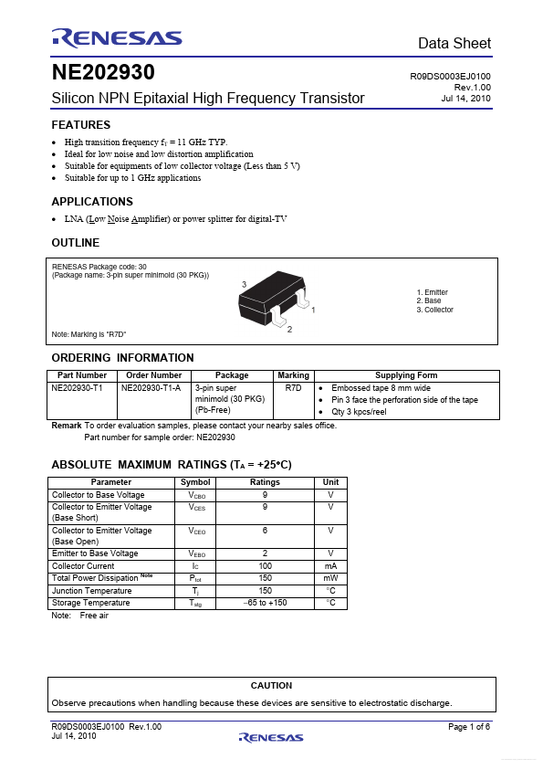
• Part: NE202930
  • Description: Silicon NPN Epitaxial High Frequency Transistor
  • Category: Transistor
  • Manufacturer: Renesas
  • Size: 230.92 KB
Download NE202930 Datasheet PDF
Renesas
NE202930
NE202930 is Silicon NPN Epitaxial High Frequency Transistor manufactured by Renesas.
FEATURES - - - - High transition frequency f T = 11 GHz TYP. Ideal for low noise and low distortion amplification Suitable for equipments of low collector voltage (Less than 5 V) Suitable for up to 1 GHz applications R09DS0003EJ0100 Rev.1.00 Jul 14, 2010 APPLICATIONS - LNA (Low Noise Amplifier) or power splitter for digital-TV OUTLINE RENESAS Package code: 30 (Package name: 3-pin super minimold (30 PKG)) 1. Emitter 2. Base 3. Collector Note: Marking is "R7D" ORDERING INFORMATION Part Number NE202930-T1 Order Number NE202930-T1-A Package 3-pin super minimold (30 PKG) (Pb-Free) Marking R7D Supplying Form - Embossed tape 8 mm wide - Pin 3 face the perforation side of the tape - Qty 3 kpcs/reel Remark To order evaluation samples, please contact your nearby sales office. Part number for sample order: NE202930 ABSOLUTE MAXIMUM RATINGS (TA = +25°C) Parameter Collector to Base Voltage Collector to Emitter Voltage (Base Short) Collector to Emitter Voltage (Base Open) Emitter to Base Voltage Collector Current Total Power Dissipation Note Junction Temperature Storage Temperature Note: Free air Symbol VCBO VCES VCEO VEBO IC Ptot Tj Tstg Ratings 9 9 6 2 100 150 150 - 65 to +150 Unit V V V V m A m W °C °C CAUTION Observe precautions when handling because these devices are sensitive to electrostatic discharge. R09DS0003EJ0100 Rev.1.00 Jul 14, 2010 Page 1 of 6 Free Datasheet http://.. ELECTRICAL CHARACTERISTICS (TA = +25°C, unless otherwise specified) Parameter DC Characteristics Collector Cut-off Current Emitter Cut-off Current DC Current Gain RF Characteristics Gain Bandwidth Product Insertion Power Gain Noise Figure (1) Noise Figure (2) Associated Gain (1) Associated Gain (2) Reverse Transfer Capacitance Maximum Stable Power Gain Gain 1 d B pression Output Power Output 3rd Order Intercept Point Symbol ICBO IEBO h FE Note1 f T ⏐S21e⏐2 NF1 NF2 Ga1 Ga2 Cre MSG Note 3 PO (1 d B) OIP3 Note 2 Test Conditions VCB = 5 V, IE = 0 VEB = 1 V, IC = 0 VCE = 5 V, IC = 5 m A VCE =...