RJK1535DPF
RJK1535DPF is N-Channel Power MOSFET manufactured by Renesas.
- Part of the RJK1535DPE comparator family.
- Part of the RJK1535DPE comparator family.
Preliminary Datasheet
RJK1535DPJ, RJK1535DPE, RJK1535DPF
Silicon N Channel MOS FET High Speed Power Switching
Features
- Low on-resistance
- Low leakage current
- High speed switching REJ03G0479-0300 Rev.3.00 Jun 30, 2010
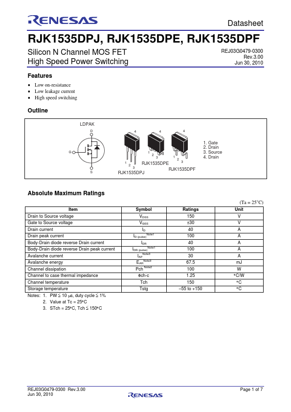
Outline
LDPAK
D 4 4 4
G 1
3 RJK1535DPE 3 RJK1535DPF RJK1535DPJ 2
1. Gate 2. Drain 3. Source 4....