• Part: R2A20121SP
  • Description: Synchronous Phase Shift Full-Bridge Controller
  • Manufacturer: Renesas
  • Size: 324.27 KB
Download R2A20121SP Datasheet PDF
Renesas
R2A20121SP
R2A20121SP is Synchronous Phase Shift Full-Bridge Controller manufactured by Renesas.
Features - - - - - 
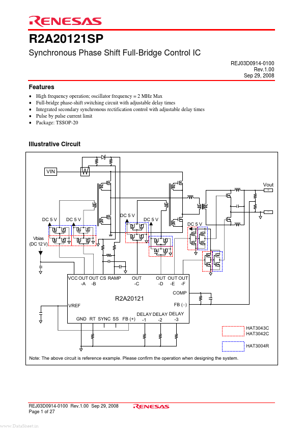
High frequency operation; oscillator frequency = 2 MHz Max Full-bridge phase-shift switching circuit with adjustable delay times Integrated secondary synchronous rectification control with adjustable delay times Pulse by pulse current limit Package: TSSOP-20 Illustrative Circuit VIN Vout + DC 5 V DC 5 V DC 5 V DC 5 V DC 5 V Vbias (DC 12 V) - VCC OUT OUT CS RAMP -A -B OUT -C OUT OUT OUT -D -E -F P R2A20121 VREF GND RT SYNC SS FB (+) FB (- ) DELAY DELAY DELAY -3 -1 -2 HAT3043C HAT3042C HAT3004R Note: The above circuit is reference example. Please confirm the operation when designing the system. REJ03D0914-0100 Rev.1.00 Sep 29, 2008 Page 1 of 27 .Data Sheet.in Pin Arrangement SYNC RAMP CS P FB (+) FB (- ) SS DELAY-1 DELAY-2 DELAY-3 1 2 3 4 5 6 7 8 9 10 (Top view) 20 19 18 17 16 15 14 13 12 11 RT GND OUT-A OUT-B OUT-C OUT-D OUT-E OUT-F VCC VREF Pin Functions Pin No. 1 2 3 4 5 6 7 8 9 10 11 12 13 14 15 16 17 18 19 20 Pin Name SYNC RAMP CS P FB (+) FB (- ) SS DELAY-1 DELAY-2 DELAY-3 VREF VCC OUT-F OUT-E OUT-D OUT-C OUT-B OUT-A GND RT Function Synchronization I/O for the oscillator Current sense signal input for the full-bridge control loop Current sense signal input for OCP Error amplifier output Error amplifier plus input Error amplifier minus input Timing capacitor for soft-start Delay time adjustor for the full-bridge control signal (OUT-A and B) Delay time adjustor for the full-bridge control signal (OUT-C and D) Delay time adjustor for the secondary control signal (OUT-E and F) 5 V/20 m A Output IC power supply input Secondary control signal Secondary control signal Full-bridge control signal Full-bridge control signal Full-bridge control signal Full-bridge control signal Ground level for the IC Timing resistor for the oscillator REJ03D0914-0100 Rev.1.00 Sep 29, 2008 Page 2 of 27 .Data Sheet.in Block Diagram H UVLO L VCC > 8.4 V→High 5V GENERATOR VREF H GOOD L VREF > 4.6 V→High VREF VREF RT Current...