RD74LVC1G08 Overview
Description
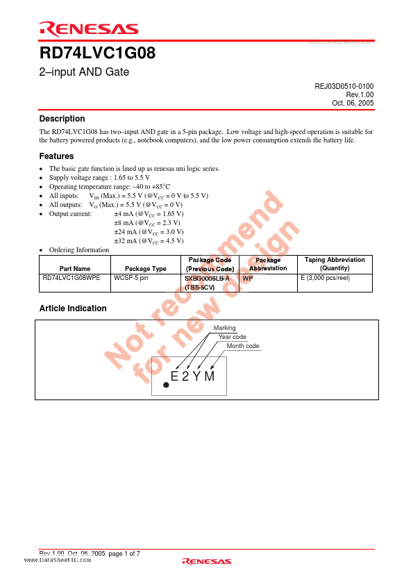
The RD74LVC1G08 has two–input AND gate in a 5-pin package. Low voltage and high-speed operation is suitable for the battery powered products (e.g., notebook computers), and the low power consumption extends the battery life.
Key Features
- The basic gate function is lined up as renesas uni logic series