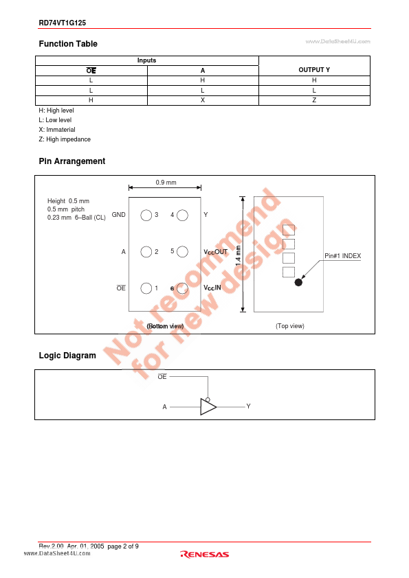
RD74VT1G125 Description
The RD74VT1G125 has a bus buffer gate with 3 state output in a 6 pin package. Output is disabled when the associated output enable (OE) input is high. To ensure the high impedance state during power up or power down, OE should be connected to VCCIN through a pull-up resistor, the minimum value of the resistor is determined by the current sinking capability of the driver.
RD74VT1G125 Key Features
- This product function as level shift that change VCCIN input level to VCCOUT output level by providing different supply
- Supplied on emboss taping for high-speed automatic mounting
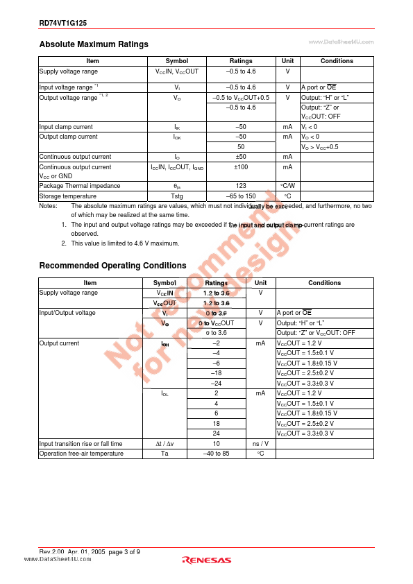
- Supply voltage range: VCCIN = 1.2 V to 3.6 V VCCOUT = 1.2 V to 3.6 V
- Operating temperature range: -40°C to +85°C
- All inputs VIH(Max.) = 3.6 V (@VCCIN = 0 V to 3.6 V) Outputs VO(Max.) = 3.6 V (@VCCOUT = 0 V)
- Ordering Information