RT9002A
RT9002A is (RT9002x) Dual Low-Dropout Regulator manufactured by Richtek.
Description
The RT9002A/B/C is a dual-channel, low noise, and low dropout regulator. The first regulator is capable of sourcing 240m A, while the second regulator can source up to 500m A and includes a voltage detection function. The RT9002A/B/C performance is optimized for CD/DVD-ROM, CD/RW or wireless munication supply applications. .. The RT9002A/B/C regulator is stable with output capacitors as low as 1μF. The other features include high output accuracy, ultra-fast transient response, tight load and line regulation, current limiting/thermal protection and high ripple rejection ratio. The RT9002A/B/C is available in SOP-8 package requiring minimum board space and smallest ponents.
Features z z z z z z z
Low Quiescent Current (Typically 70μA) Wide Operating Voltage Ranges : 2.5V to 5.5V Ultra-Fast Transient Response Tight Load and Line Regulation Current Limiting Protection Thermal Shutdown Protection Only low-ESR Ceramic Capacitors Required for Stability Custom LDO VOUT1, VOUT2 Voltage Available from 1.5V to 3.3V Custom VIN Detector Available from 3.5V to 4.0V Ro HS pliant and 100% Lead (Pb)-Free z z z
Applications Ordering Information
RT9002A/B/C Package Type S : SOP-8 Operating Temperature Range P : Pb Free with mercial Standard G : Green (Halogen Free with mercial Standard) Output Voltage : VOUT1/VOUT2 A : 2.5V/3.3V B : 1.5V/2.8V C : 2.5V/3.3V z z z z
CD/DVD-ROM, CD/RW Wireless LAN Card/Keyboard/Mouse Battery-Powered Equipment XDSL Router
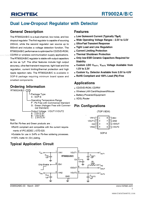
Pin Configurations
(TOP VIEW)
VIN1 VOUT1 Cd VIN2 2 3 4 8 7 6 5 EN1 GND VDOUT VOUT2
Note :
Rich Tek Pb-free and Green products are :
`Ro HS pliant and patible with the current requirements of IPC/JEDEC J-STD-020.
`Suitable for use in Sn Pb or Pb-free soldering processes. `100% matte tin (Sn) plating.
SOP-8
Typical Application Circuit
VIN1 1 CIN1 1u F 8 VIN1 VOUT1 2 3 Cd 6 5 COUT2 1u F COUT1 1u F R1 100k VOUT1
RT9002A/B/C Cd EN1 VDOUT
Chip Enable
VIN2 VDOUT VOUT2
VIN2
4 CIN2 1u F
VIN2 GND 7
VOUT2
DS9002ABC-03 March...