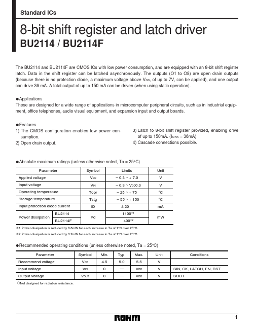
BU2114
Features
- 1) The CMOS configuration enables low power consumption. 2) Open drain output.
3) Latch to 8-bit shift register provided, enabling drive of up to 150m A. (ISINK = 36m A) 4) Cascade connections possible.
- Absolute maximum ratings (unless otherwise noted, Ta = 25°C)
Parameter Applied voltage Input voltage Operating temperature Storage temperature Input protection diode current Power dissipation BU2114 BU2114F Symbol VDD VIN Topr Tstg ID Pd Limits
- 0.3 ~ + 7.0
- 0.3 ~ VDD0.3
- 25 ~ + 75
- 55 ~ + 150 ± 20 1100∗1 400∗2 Unit V V °C °C m A m W
∗1 Power dissipation is reduced by 8.8m W for each increase in Ta of 1°C over 25°C. ∗2 Power dissipation is reduced by 3.2m W for each increase in Ta of 1°C over 25°C.
- Remended operating conditions (unless otherwise noted, Ta = 25°C)
Parameter Remend voltage Input voltage Output voltage
᭺Not designed for radiation resistance.
Symbol VDD VIN VOUT
Min. 4.5 0 0
Typ. 5.0
- -
Max. 5.5 VDD VDD
Unit V V V
Conditions
SIN, CK, LATCH, EN, RST...