Datasheet Details
| Part number | R5011FNX |
|---|---|
| Manufacturer | ROHM |
| File Size | 708.16 KB |
| Description | Nch 500V 11A Power MOSFET |
| Datasheet | R5011FNX-Rohm.pdf |
|
|
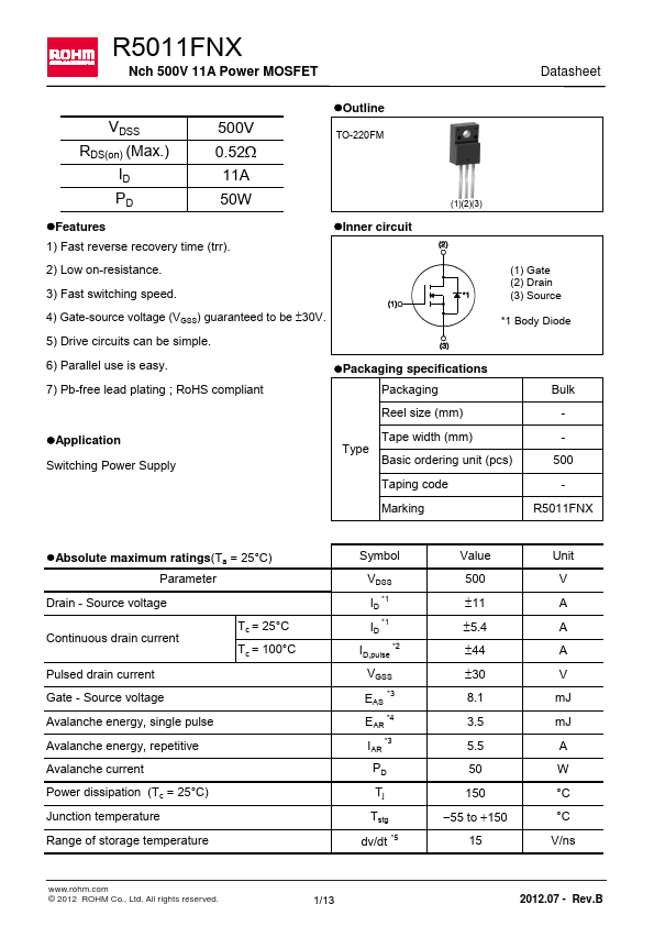
Overview: R5011FNX Nch 500V 11A Power MOSFET Datasheet VDSS RDS(on) (Max.) ID PD 500V 0.
| Part number | R5011FNX |
|---|---|
| Manufacturer | ROHM |
| File Size | 708.16 KB |
| Description | Nch 500V 11A Power MOSFET |
| Datasheet | R5011FNX-Rohm.pdf |
|
|
|
| Brand Logo | Part Number | Description | Manufacturer |
|---|---|---|---|
| R5011010 | General Purpose Rectifier | Powerex Power Semiconductors | |
| R5011015 | General Purpose Rectifier | Powerex Power Semiconductors | |
| R5011210 | General Purpose Rectifier | Powerex Power Semiconductors | |
| R5011215 | General Purpose Rectifier | Powerex Power Semiconductors | |
| R5011410 | General Purpose Rectifier | Powerex Power Semiconductors |
| Part Number | Description |
|---|---|
| R5011ANJ | Nch 500V 11A Power MOSFET |
| R5011ANX | 10V Drive Nch MOSFET |
| R5013ANJ | Nch 500V 13A Power MOSFET |
| R5013ANX | 10V Drive Nch MOSFET |
| R5016ANJ | Nch 500V 16A Power MOSFET |
| R5016ANX | Nch 500V 16A Power MOSFET |
| R5019ANJ | 10V Drive Nch MOSFET |
| R5019ANX | 10V Drive Nch MOSFET |
| R5005CNJ | 10V Drive N-channel MOSFET |
| R5007ANJ | 10V Drive Nch MOSFET |