RJK005N03
Key Features
- 8 (2) (1)
- 6 2.8
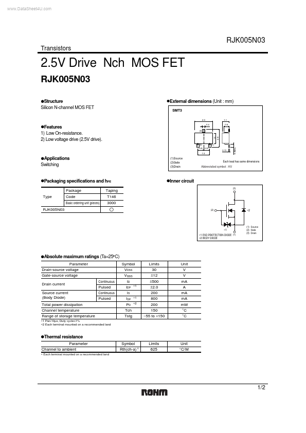
- 95 0.95 0.15 1.9 zApplications Switching zPackaging specifications and hFE Package Type RJK005N03 Code Basic ordering unit (pieces) Taping T146 3000 (1)Source (2)Gate (3)Drain Each lead has same dimensions Abbreviated symbol : KV zInner circuit (3)
- 3Min. (2) ∗2 ∗1 ∗1 ESD PROTECTION DIODE (1) ∗2 BODY DIODE (1) Source (2) Gate (3) Drain zAbsolute maximum ratings (Ta=25°C) Parameter Drain-source voltage Gate-source voltage Drain current Source current (Body Diode) Continuous Pulsed Continuous Pulsed Total power dissipation Channel temperature Range of storage temperature ∗1 Pw≤10µs, Duty cycle≤1% ∗2 Each terminal mounted on a recommended land Symbol VDSS VGSS ID IDP ∗1 IS ISP ∗1 PD ∗2 Tch Tstg Limits 30 ±12 ±500 ±2.0 200 800 200 150 -55 to +150 Unit V V mA A mA mA mW °C °C zThermal resistance Parameter Channel to ambient ∗ Each terminal mounted on a recommended land Symbol Rth(ch-a) ∗ Limits 625 Unit °C/W 1/2