MM1W10
Key Features
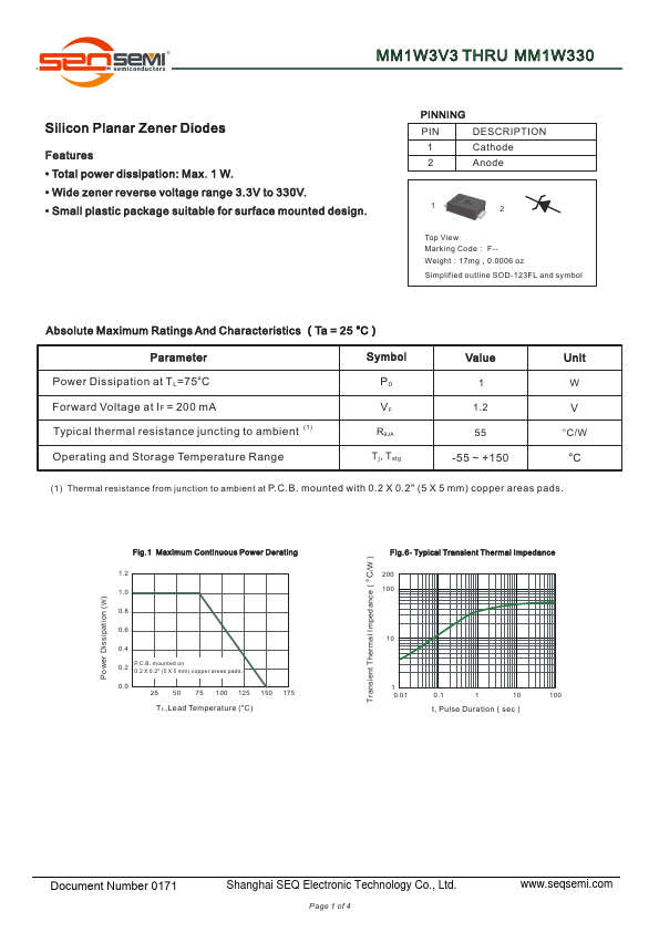
- Total power dissipation: Max. 1 W.
- Wide zener reverse voltage range 3.3V to 330V.
- Small plastic package suitable for surface mounted design.
| Part Number | Manufacturer | Description |
|---|---|---|
| MM1W100 | AiT Components | ZENER DIODE |
| MM1W10 | AiT Components | ZENER DIODE |
| MM1W100L | Jingdao Microelectronics | Silicon Planar Zener Diodes |
| MM1W110 | Jingdao Microelectronics | Silicon Planar Zener Diodes |
| MM1W180 | Jingdao Microelectronics | Silicon Planar Zener Diodes |
| MM1W150 | Jingdao Microelectronics | Silicon Planar Zener Diodes |
| MM1W165 | Jingdao Microelectronics | Silicon Planar Zener Diodes |
| MM1W16 | Jingdao Microelectronics | Silicon Planar Zener Diodes |
| MM1W12 | Jingdao Microelectronics | Silicon Planar Zener Diodes |
| MM1W180 | AiT Components | ZENER DIODE |