Datasheet Summary
..
S71WS512N to S71WS512P
Migrating from the S71WS512N to the S71WS512P
Application Note by Daisuke Nakata
1. Introduction
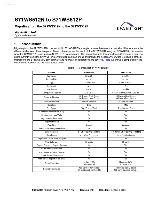
Migrating from the S71WS512N to the monolithic S71WS512P is a simple process; however, the user should be aware of a few differences between these two parts. These differences are the result of the S71WS512N using two S29WS256N die in series while the S71WS512P uses a single S29WS512P configuration. This application note describes these differences in detail so users currently using the S71WS512N configuration can plan ahead and include the necessary software to ensure a smooth migration to the S71WS512P. Both software and hardware considerations are...