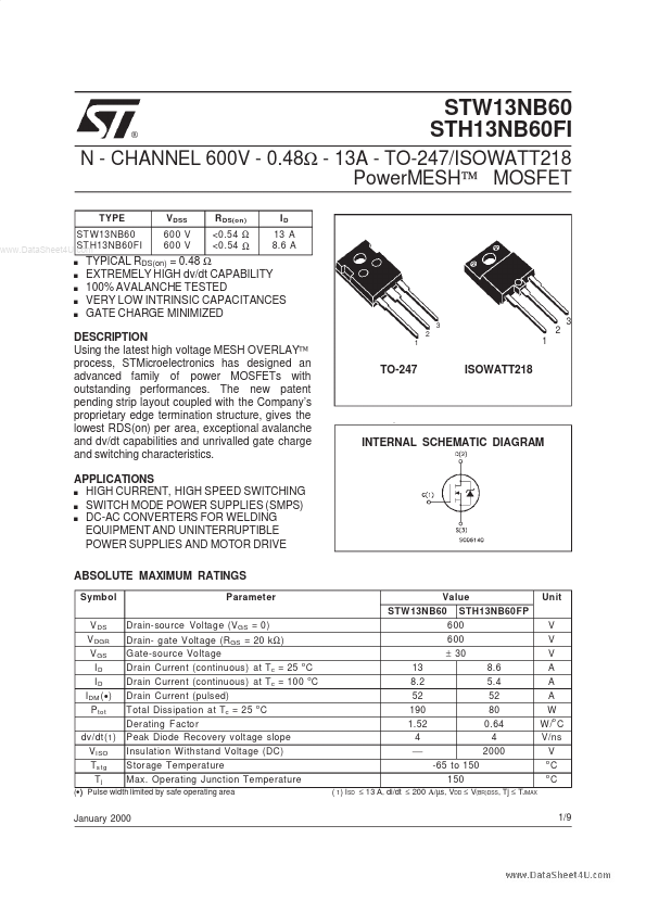
Datasheet4U Logo Datasheet4U.com

13NB60 - STW13NB60

General Description

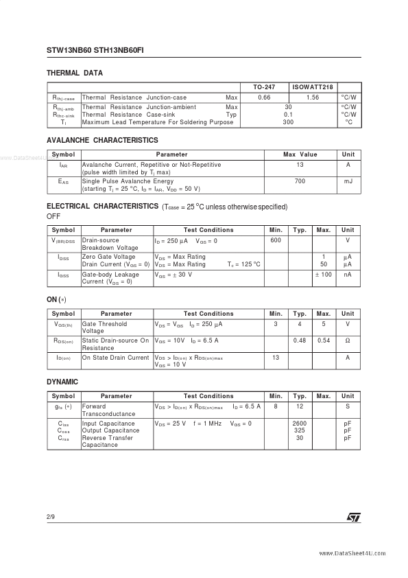
Using the latest high voltage MESH OVERLAY™ process, STMicroelectronics has designed an advanced family of power MOSFETs with outstanding performances.

The new patent pending strip layout coupled with the Company’s proprietary edge termination structure, gives the lowest RDS(on) per area, exceptional avalanche and dv/dt capabilities and unrivalled gate charge and switching characteristics.

APPLICATIONS s HIGH CURRENT, HIGH SPEED SWITCHING s SWITCH MODE POWER SUPPLIES (SMPS) s DC-AC CONVERTERS FOR WELDING EQUIPMENT AND UNINTERRUPTIBLE POWER SUPPLIES AND MOTOR DRIVE 3 2 1 TO-247 3 2 1 ISOWATT218 INTERNAL SCHEMATIC DIAGRAM ABSOLUTE MAXIMUM RATINGS Sy mb o l Parameter VDS Drain-source Voltage (VGS = 0) VDGR Drain- gate Voltage (RGS = 20 kΩ) VGS Gate-source Voltage ID Drain Current (continuous) at Tc = 25 oC ID Drain Current (continuous) at Tc = 100 oC IDM (•) Drain Current (pulsed) Ptot Total Dissipation at Tc = 25 oC Derating Factor dv/dt(1) Peak Diode Recovery voltage slope VISO I nsulat ion W ithstand Voltage (DC) Tstg Storage Temperature Tj Max.

Overview

STW13NB60 ® STH13NB60FI N - CHANNEL 600V - 0.48Ω - 13A - TO-247/ISOWATT218 PowerMESH™ MOSFET TYPE VDSS RDS(on) ID ST W13 NB6 0 600 V <0.54 Ω 13 A www.DataSheet4U.cSoTmH13 NB 6 0F I 600 V <0.54 Ω 8.6 A s TYPICAL RDS(on) = 0.