74ACT74
74ACT74 is Dual D-Type Flip-Flop manufactured by STMicroelectronics.
DESCRIPTION
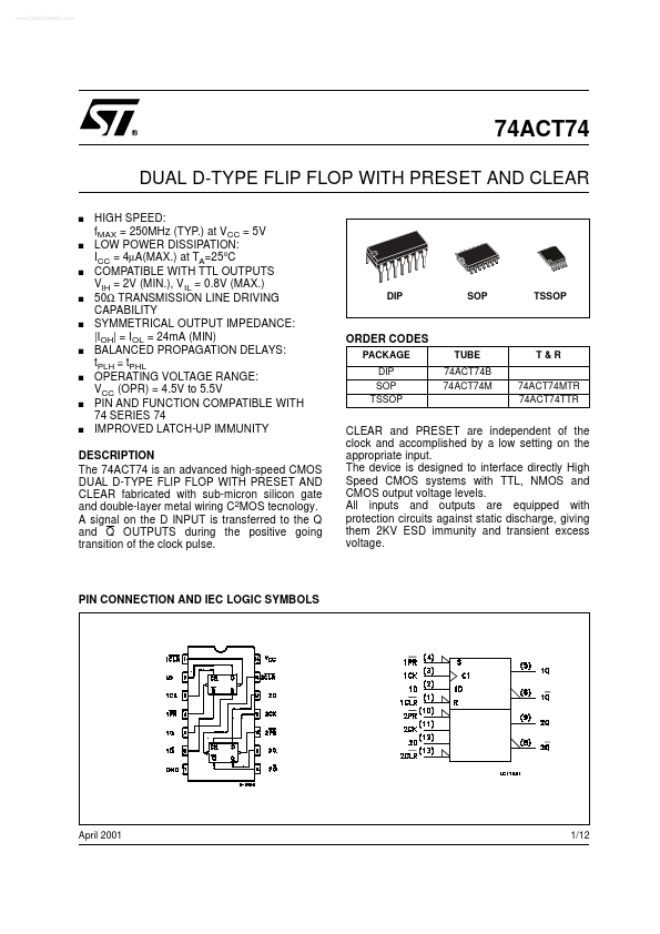
The 74ACT74 is an advanced high-speed CMOS DUAL D-TYPE FLIP FLOP WITH PRESET AND CLEAR fabricated with sub-micron silicon gate and double-layer metal wiring C2MOS tecnology. A signal on the D INPUT is transferred to the Q and Q OUTPUTS during the positive going transition of the clock pulse.
CLEAR and PRESET are independent of the clock and acplished by a low setting on the appropriate input. The device is designed to interface directly High Speed CMOS systems with TTL, NMOS and CMOS output voltage levels. All inputs and outputs are equipped with protection circuits against static discharge, giving them 2KV ESD immunity and transient excess voltage.
PIN CONNECTION AND IEC LOGIC SYMBOLS
April 2001
1/12
INPUT AND OUTPUT EQUIVALENT CIRCUIT PIN DESCRIPTION
PIN No 1, 13 2, 12 3, 11 SYMBOL 1CLR, 2CLR 1D, 2D 1CK, 2CK NAME AND FUNCTION Asyncronous Reset Direct Input Data Inputs Clock Input (LOW to HIGH, Edge Triggered) Asyncronous Set
- Direct Input True Flip-Flop Outputs plement Flip-Flop Outputs Ground (0V) Positive Supply Voltage
4, 10 5, 9 6, 8 7 14
1PR, 2PR 1Q, 2Q 1Q, 2Q GND VCC
TRUTH TABLE
INPUTS CLR L H L H H H
X : Don’t Care
OUTPUTS FUNCTION D X X X L H X CK X X X Q L H H L H Qn Q L L H H L Qn NO CHANGE CLEAR PRESET
PR H L L H H H
LOGIC DIAGRAM
This logic diagram has not be used to estimate propagation delays
2/12
ABSOLUTE MAXIMUM RATINGS
Symbol VCC VI VO IIK IOK IO Tstg TL Supply Voltage DC Input Voltage DC Output Voltage DC Input Diode Current DC Output Diode Current DC Output Current Storage Temperature Lead Temperature (10 sec) Parameter Value -0.5 to +7 -0.5 to VCC + 0.5 -0.5 to VCC + 0.5 ± 20 ± 20 ± 50 ± 200 -65 to +150 300 Unit V V V m A m A m A m A °C °C
ICC or IGND DC VCC or Ground Current
Absolute Maximum Ratings are those values beyond which damage to the device may occur. Functional operation under these conditions is not implied.
REMENDED OPERATING CONDITIONS
Symbol VCC VI VO Top dt/dv Supply Voltage Input...