BN15D100
Features
- Good h FE linearity
- High f T frequency
- Monolithic Darlington configuration with integrated antiparallel collector-emitter diode
Application
- Linear and switching industrial equipment
Description
The device is manufactured in planar technology with “base island” layout and monolithic Darlington configuration.
3 1
D²PAK
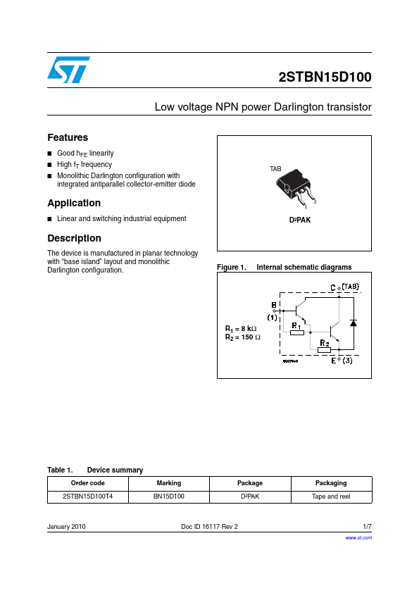
Figure 1. Internal schematic diagrams
R1 = 8 kΩ R2 = 150 Ω
Table 1. Device summary Order code
2STBN15D100T4
Marking BN15D100
Package D²PAK
January 2010
Doc ID 16117 Rev 2
Packaging Tape and reel
1/7
.st.
Electrical ratings
Electrical ratings
Table 2. Absolute maximum ratings
Symbol
Parameter
VCBO VCEO VEBO
IC ICM IB PTOT TSTG TJ
Collector-base voltage (IE = 0) Collector-emitter voltage (IB = 0) Emitter-base voltage (IC = 0) Collector current Collector peak current Base current Total dissipation at Tcase = 25 °C Storage temperature Max. operating junction temperature
Table 3. Thermal data
Symbol
Parameter
Rth JC Thermal...