Datasheet4U Logo Datasheet4U.com

LCX125Y - Low-voltage CMOS quad bus buffer

Download the LCX125Y datasheet PDF (LCX125 included). The manufacturer datasheet provides complete specifications, pinout details, electrical characteristics, and typical applications for low-voltage cmos quad bus buffer.

Description

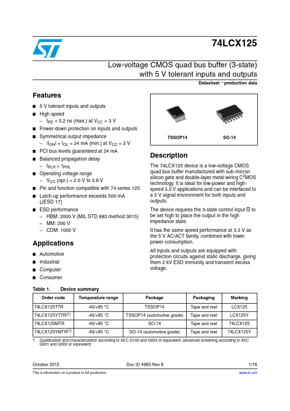
The 74LCX125 device is a low-voltage CMOS quad bus buffer manufactured with sub-micron silicon gate and double-layer metal wiring C2MOS technology.

It is ideal for low-power and highspeed 3.3 V applications and can be interfaced to a 5 V signal environment for both inputs and outputs.

Features

  • 5 V tolerant inputs and outputs.
  • High speed.
  • tPD = 5.2 ns (max. ) at VCC = 3 V.
  • Power-down protection on inputs and outputs.
  • Symmetrical output impedance.
  • |IOH| = IOL = 24 mA (min. ) at VCC = 3 V.
  • PCI bus levels guaranteed at 24 mA.
  • Balanced propagation delay.
  • tPLH ≅ tPHL.
  • Operating voltage range.
  • VCC (opr. ) = 2.0 V to 3.6 V.
  • Pin and function compatible with 74 series 125.
  • Latch-up performance exceeds 500 mA (JESD 17.

📥 Download Datasheet

Note: The manufacturer provides a single datasheet file (LCX125-STMicroelectronics.pdf) that lists specifications for multiple related part numbers.
Other Datasheets by STMicroelectronics

Full PDF Text Transcription

Click to expand full text
74LCX125 Low-voltage CMOS quad bus buffer (3-state) with 5 V tolerant inputs and outputs Datasheet −production data Features ■ 5 V tolerant inputs and outputs ■ High speed – tPD = 5.2 ns (max.) at VCC = 3 V ■ Power-down protection on inputs and outputs ■ Symmetrical output impedance – |IOH| = IOL = 24 mA (min.) at VCC = 3 V ■ PCI bus levels guaranteed at 24 mA ■ Balanced propagation delay – tPLH ≅ tPHL ■ Operating voltage range – VCC (opr.) = 2.0 V to 3.
Published: |