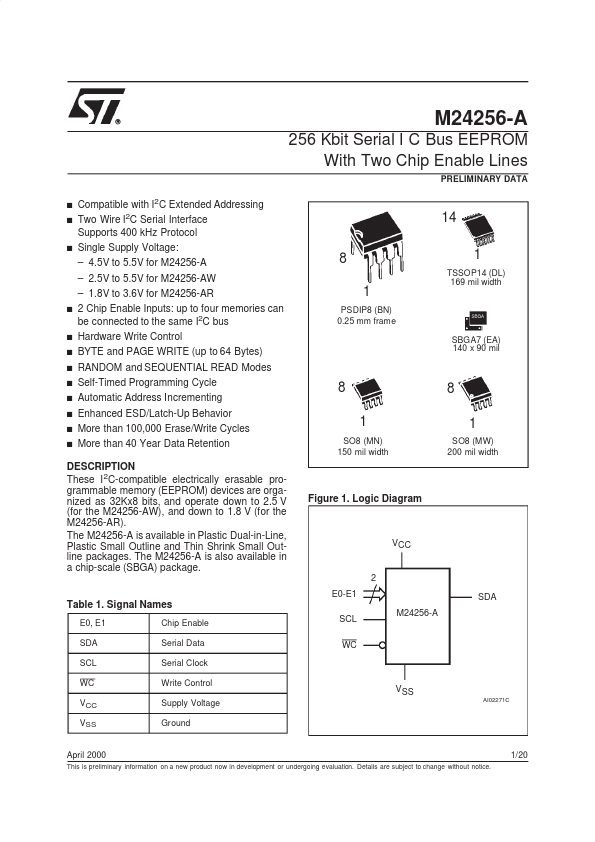
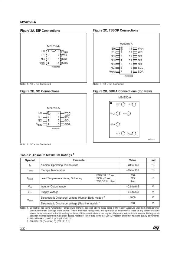
M24256-A
256 Kbit Serial I C Bus EEPROM
With Two Chip Enable Lines
PRELIMINARY DATA
s Compatible with I2C Extended Addressing
s Two Wire I2C Serial Interface
Supports 400 kHz Protocol
s Single Supply Voltage:
– 4.5V to 5.5V for M24256-A
– 2.5V to 5.5V for M24256-AW
– 1.8V to 3.6V for M24256-AR
s 2 Chip Enable Inputs: up to four memories can
be connected to the same I2C bus
s Hardware Write Control
s BYTE and PAGE WRITE (up to 64 Bytes)
s RANDOM and SEQUENTIAL READ Modes
s Self-Timed Programming Cycle
s Automatic Address Incrementing
s Enhanced ESD/Latch-Up Behavior
s More than 100,000 Erase/Write Cycles
s More than 40 Year Data Retention
DESCRIPTION
These I2C-compatible electrically erasable pro-
grammable memory (EEPROM) devices are orga-
nized as 32Kx8 bits, and operate down to 2.5 V
(for the M24256-AW), and down to 1.8 V (for the
M24256-AR).
The M24256-A is available in Plastic Dual-in-Line,
Plastic Small Outline and Thin Shrink Small Out-
line packages. The M24256-A is also available in
a chip-scale (SBGA) package.
Table 1. Signal Names
E0, E1
Chip Enable
SDA
Serial Data
SCL
Serial Clock
WC Write Control
VCC
VSS
Supply Voltage
Ground
8
1
PSDIP8 (BN)
0.25 mm frame
8
1
SO8 (MN)
150 mil width
14
1
TSSOP14 (DL)
169 mil width
SBGA
SBGA7 (EA)
140 x 90 mil
8
1
SO8 (MW)
200 mil width
Figure 1. Logic Diagram
VCC
2
E0-E1
SCL
WC
M24256-A
SDA
VSS
AI02271C
April 2000
This is preliminary information on a new product now in development or undergoing evaluation. Details are subject to change without notice.
1/20