M24512
Description
M24512 is a 512-Kbit I2C-compatible EEPROM (electrically erasable programmable memory) organized as 64 K × 8 bits. The M24512-W can operate with a supply voltage from 2.5 V to 5.5 V, the M24512-R can operate with a supply voltage from 1.8 V to 5.5 V, and the M24512-DF can operate with a supply voltage from 1.7 V to 5.5 V.
Key Features
- compatible with following I2C bus modes: – 1 MHz – 400 kHz – 100 kHz
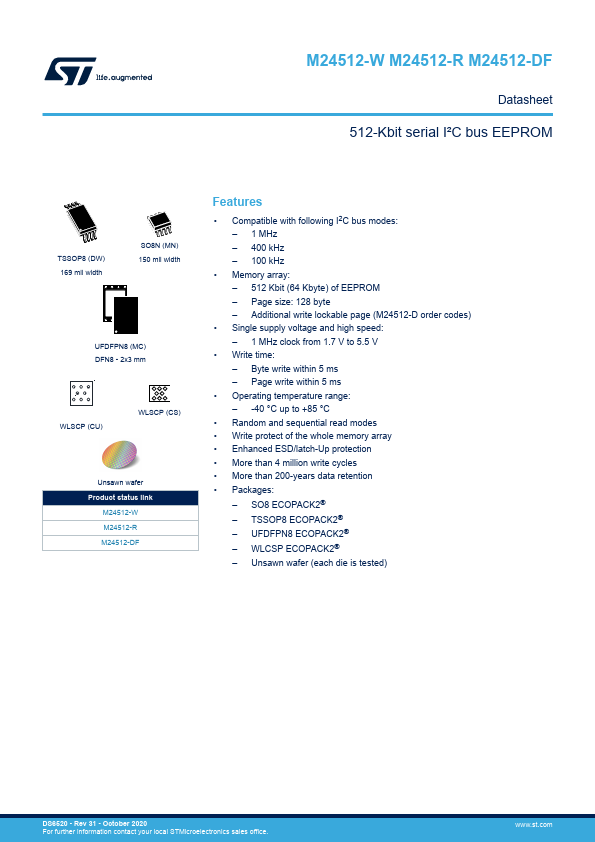
- Memory array: – 512 Kbit (64 Kbyte) of EEPROM – Page size: 128 byte – Additional write lockable page (M24512-D order codes)
- Single supply voltage and high speed: – 1 MHz clock from 1.7 V to 5.5 V
- Write time: – Byte write within 5 ms – Page write within 5 ms
- Operating temperature range: – -40 °C up to +85 °C
- Random and sequential read modes
- Write protect of the whole memory array
- Enhanced ESD/latch-Up protection
- More than 4 million write cycles
- More than 200-years data retention