STF25NM60N
STF25NM60N is N-CHANNEL MOSFET manufactured by STMicroelectronics.
STB25NM60Nx
- STF25NM60N STP25NM60N
- STW25NM60N
N-channel 600 V, 0.130 Ω , 21 A, MDmesh™ II Power MOSFET
..
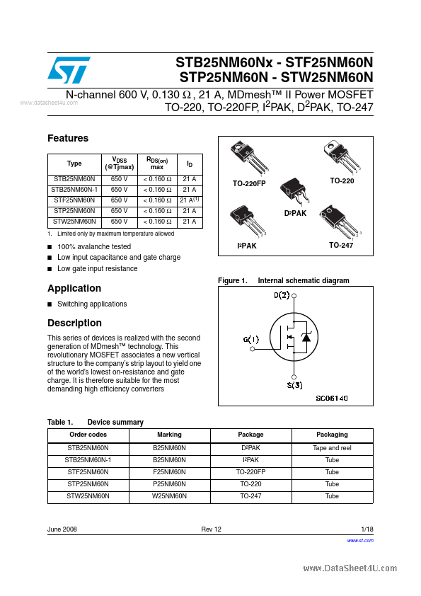
TO-220, TO-220FP, I2PAK, D2PAK, TO-247
Features
Type
VDSS (@Tjmax)
RDS(on) max
STB25NM60N STB25NM60N-1 STF25NM60N STP25NM60N STW25NM60N
650 V 650 V 650 V 650 V 650 V
< 0.160 Ω < 0.160 Ω < 0.160 Ω < 0.160 Ω < 0.160 Ω
21 A 21 A 21 A(1) 21 A 21 A
1. Limited only by maximum temperature allowed
- 100% avalanche tested
- Low input capacitance and gate charge
- Low gate input resistance
Application
- Switching applications
Description
This series of devices is realized with the second generation of MDmesh™ technology. This revolutionary MOSFET associates a new vertical structure to the pany’s strip layout to yield one of the world’s lowest on-resistance and gate charge. It is therefore suitable for the most demanding high efficiency converters
3 2 1
TO-220FP
3 1
D²PAK
I²PAK
3 2 1
TO-220
3 2...