Datasheet Summary
..
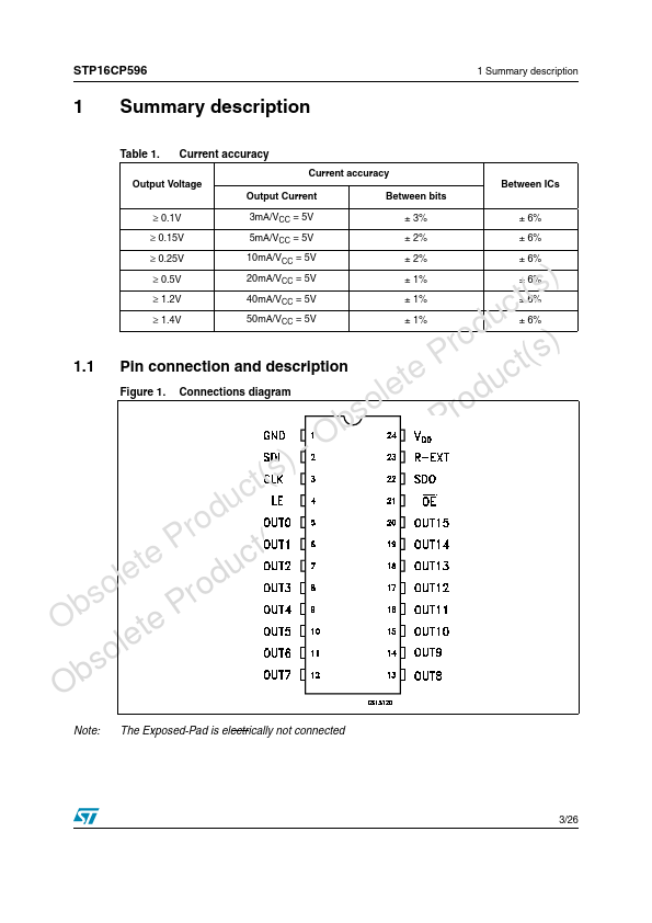
Table 2: Typical Current Accuracy
Output Voltage ≥ 0.1V ≥ 0.15V ≥ 0.25V ≥ 0.5V ≥ 1.2V ≥ 1.4V Output Current 3 mA/VCC = 5V 5 mA/VCC = 5V 10 mA/VCC = 5V 20 mA/VCC = 5V 40 mA/VCC = 5V 50 mA/VCC = 5V Between Bits ± 3% ± 2% ± 2% ± 1% ± 1% ± 1% Between ICs ± 6% ± 6% ± 6% ± 6% ± 6% ± 6%
Figure 1: Pin Connection (Note 1)
Note 1: The exposed Pad is electrically not connected.
Table 3: Pin Description
PIN N° 1 2 3 4 5-20 21 22 23 24 Symbol GND SDI CLK /LE OUT 0-15 /OE SDO R-EXT VDD Name and Function Ground Terminal Serial data input terminal Clock input terminal Latch input terminal Output terminal Input terminal of output enable (active low) Serial data out...