STSA1805
DESCRIPTION
The device is manufactured in NPN Planar Technology by using a "Base Island" layout. The resulting Transistor shows exceptional high gain performance coupled with very low saturation voltage.
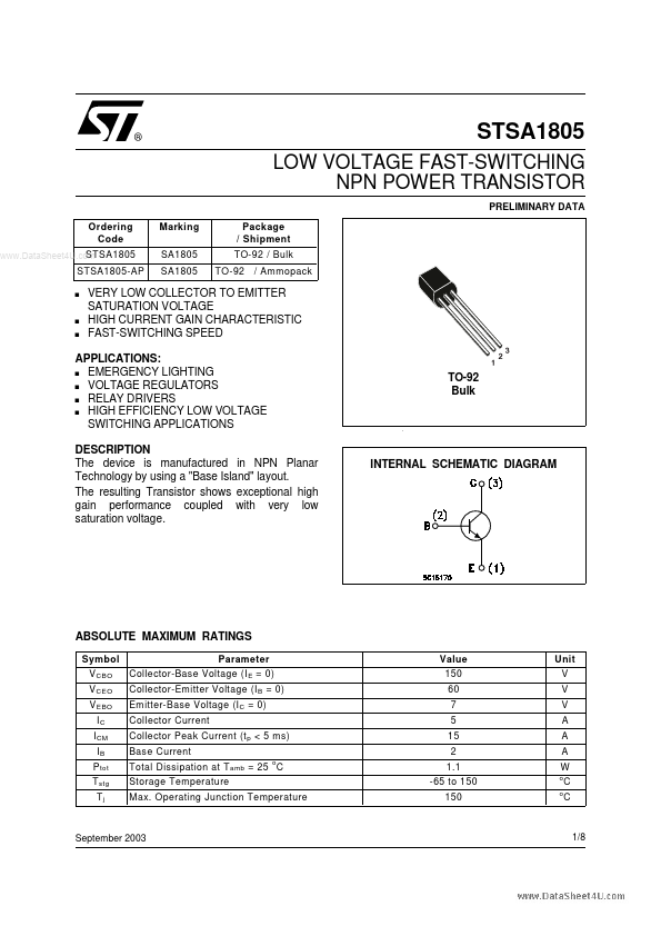
INTERNAL SCHEMATIC DIAGRAM
ABSOLUTE MAXIMUM RATINGS
Symbol V CBO V CEO V EBO IC I CM IB P tot T stg Tj Parameter Collector-Base Voltage (I E = 0) Collector-Emitter Voltage (I B = 0) Emitter-Base Voltage (I C = 0) Collector Current Collector Peak Current (t p < 5 ms) Base Current Total Dissipation at T amb = 25 o C Storage Temperature Max. Operating Junction Temperature Value 150 60 7 5 15 2 1.1 -65 to 150 150 Unit V V V A A A W o o
September 2003
1/8
THERMAL DATA
R thj-amb R thj-case Thermal Resistance Junction-Ambient Thermal Resistance Junction-case Max Max 114 83.3 o o
C/W C/W
ELECTRICAL CHARACTERISTICS (Tcase = 25 o C unless otherwise specified)
Symbol I CBO I EBO Parameter Collector Cut-off Current (I E = 0) Emitter Cut-off Current (I C = 0) Collector-Base...