TDA2270
TDA2270 is TV VERTICAL DEFLECTION OUTPUT CIRCUIT manufactured by STMicroelectronics.
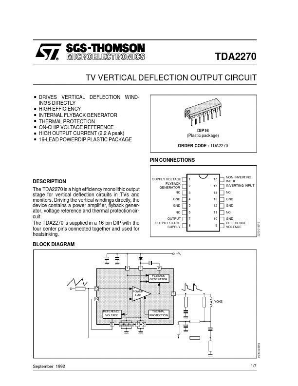
DESCRIPTION
The TDA2270 is a high efficiency monolithic output stage for vertical deflection circuits in TVs and monitors. Driving the vertical windings directly, the device contains a power amplifier, flyback generator, voltage reference and thermal protection circuit. The TDA2270 is supplied in a 16-pin DIP with the four center pins connected together and used for heatsinking. BLOCK DIAGRAM
SUPPLY VOLTAGE FLYBACK GENERATOR NC GND GND NC OUTPUT OUTPUT STAGE SUPPLY
1 2 3 4 5 6 7 8
16 15
NON-INVER TING INPUT INVERTING INPUT NC GND GND NC
2270-01.EPS
13 12 11 10 9
GND REFERENCE VOLTAGE
+VS
FLYBACK GENERATOR
POWER AMP.
7 YOKE
REFER ENCE VOLTAGE
THERMAL PROTECTION 4
12 13 10
September 1992
1/7
2270-02.EPS
ABSOLUTE MAXIMUM RATINGS
Symbol Vs V7 , V8 V2 V15, V16 Io Io Io I2 I2 Ptot Tstg, Tj Supply Voltage (pin 1) Flyback Peak Voltage Voltage at Pin 2 Amplifier Input Voltage Output Peak Current (non repetitive, t = 2 ms) Output Peak Current at f = 50 Hz, t ≤ 10 µs Output Peak Current at f = 50 Hz, t > 10 µs Pin 2 DC Current at V7 < V1 Pin 2 Peak to Peak Flyback Current at f = 50 Hz, tfly ≤ 1.5 ms Total Power Dissipation at Tpins ≤ 90 °C Tamb = 70 °C Parameter Value 35 60 + Vs + Vs,
- 0.5 2 2.2 1.2 50 2 4.3 1
- 40 to 150 V A A A m A A
2270-01.TBL 2270-03.TBL 2270-02.TBL
Unit V V
W W °C
Storage and Junction Temperature
THERMAL DATA
Symbol Rth j- case R th j- amb Parameter Thermal Resistance Junction-case Thermal Resistance Junction- ambient Max Max Value 14 80 Unit °C/W °C/W
- Obtained with the GND pins soldered to printed circuit with minimized copper area.
ELECTRICAL CHARACTERISTICS (refer to the test circuits, VS = 35 V, Tamb = 25o C unless otherwise specified)
Symbol I1 I8 I15 I16 V2L V7 V7L V7H V9 ∆ V9 ∆ VS R9 Tj Parameter Pin 1 Quiescent Current Pin 8 Quiescent Current Amplifier Input Bias Current Amplifier Input Bias Current Pin 2 Saturation Voltage to GND Quiescent Output Voltage Output Saturation Voltage to GND...