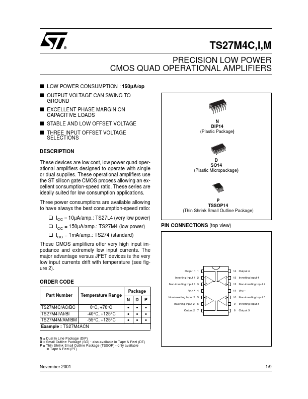
TS27M4AC
TS27M4AC is PRECISION LOW POWER CMOS QUAD OPERATIONAL AMPLIFIERS manufactured by STMicroelectronics.
DESCRIPTION
These devices are low cost, low power quad operational amplifiers designed to operate with single or dual supplies. These operational amplifiers use the ST silicon gate CMOS process allowing an excellent consumption-speed ratio. These series are ideally suited for low consumption applications. Three power consumptions are available allowing to have always the best consumption-speed ratio:
N DIP14 (Plastic Package)
D SO14 (Plastic Micropackage)
P TSSOP14 (Thin Shrink Small Outline Package) u ICC = 10µA/amp.: TS27L4 (very low power) u ICC = 150µA/amp.: TS27M4 (low power) u ICC = 1m A/amp.: TS274 (standard)
These CMOS amplifiers offer very high input impedance and extremely low input currents. The major advantage versus JFET devices is the very low input currents drift with temperature (see figure 2). ORDER CODE
Package Part Number Temperature Range N TS27M4C/AC/BC 0°C, +70°C TS27M4I/AI/BI -40°C, +125°C TS27M4M/AM/BM -55°C, +125°C Example : TS27M4ACN
- -
- D
- -
- P
- -
- PIN CONNECTIONS (top view)
Output 1 1 Inverting Input 1 2 Non-inverting Input 1 3 VCC + 4 Non-inverting Input 2 5 Inverting Input 2 6 Output 2 7 + + + +
14 Output 4 13 Inverting Input 4 12 Non-inverting Input 4 11 VCC 10 Non-inverting Input 3 9 8 Inverting Input 3 Output 3
N = Dual in Line Package (DIP) D = Small Outline Package (SO)
- also available in Tape & Reel (DT) P = Thin Shrink Small Outline Package (TSSOP)
- only available in Tape & Reel (PT)
November 2001
1/9
TS27M4C,I,M
BLOCK DIAGRAM
Current source x I
Input differential
Second stage
Output stage
Output
ABSOLUTE MAXIMUM RATINGS
Symbol VCC Vid Vi Io Iin Toper Tstg
+
Parameter Supply Voltage
3) 1) 2)
TS27M4C/AC/BC
TS27M4I/AI/BI TS27M4M/AM/BM 18 ±18 -0.3 to 18 ±30 ±5
Unit V V V m A m A
Differential Input Voltage Input Voltage
Output Current for VCC+ ≥ 15V Input Current Operating Free-Air Temperature Range Storage Temperature Range 0 to +70
-40 to +125 -65 to...