TSH343
TSH343 is Single - Supply Triple Video Buffer manufactured by STMicroelectronics.
Description
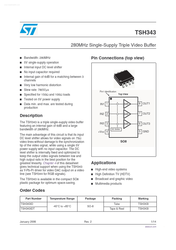
The TSH343 is a triple single-supply video buffer featuring an internal gain of 6d B and a large bandwidth of 280MHz. The main advantage of this circuit is that its input DC level shifter allows for video signals on 75Ω video lines without damage to the synchronization tip of the video signal, while using a single 5V power supply with no input capacitor. The DC level shifter is internally fixed and optimized to keep the output video signals between low and high output rails in the best position for the greatest linearity. Chapter 4 of this datasheet gives technical support when using the TSH343 as Y-Pb-Pr driver for video DAC output on a video line (see TSH344 for RGB signals). The TSH343 is available in the pact SO8 plastic package for optimum space-saving.
IN2 2
6d B
7 OUT2
IN3 3
DC Shifter
6d B
6 OUT3 5 GND
+Vcc 4
SO8
Applications
- -
- -
High-end video systems High Definition TV (HDTV) Broadcast and graphic video Multimedia products
Order Codes
Part Number TSH343ID TSH343IDT Temperature Range -40°C to +85°C Package SO-8 Packing Tube Tape & Reel Marking TSH343I TSH343I
January 2006
Rev. 2
1/14
.st.
Absolute Maximum Ratings
Table 1.
Symbol VCC Vin Toper Tstd Tj Rthjc Rthja Pmax. ESD
Absolute Maximum Ratings
Key parameters and their absolute maximum ratings
Parameter Supply voltage
(1)
Value 6 0 to +1.4 -40 to +85 -65 to +150 150 28 157 800 2 1.5 200
Unit V V °C °C °C °C/W °C/W m W k V k V V
Input Voltage Range (2) Operating Free Air Temperature Range Storage Temperature Maximum Junction Temperature SO8 Thermal Resistance Junction to Case SO8 Thermal Resistance Junction to Ambient Area Maximum Power Dissipation (@Ta=25°C) for Tj=150°C CDM: Charged Device Model HBM: Human Body Model MM: Machine Model
1. All voltage values, except differential voltage, are with respect to network terminal. 2. The magnitude of input and output voltage must never exceed VCC +0.3V.
Table 2.
Symbol VCC
Operating conditions
Parameter Power Supply...