Datasheet4U Logo Datasheet4U.com

W25NM60N - STW25NM60N

General Description

du - OThis series of devices is realized with the second ro )generation of MDmesh™ technology.

This P t(srevolutionary MOSFET associates a new vertical te cstructure to the company’s strip layout to yield one le uof the world’s lowest on-resistance and gate dcharge.

Key Features

  • Type VDSS (@Tjmax) RDS(on) max ID STB25NM60N t(s)STB25NM60N-1 cSTF25NM60N uSTP25NM60N rod )STW25NM60N 650 V 650 V 650 V 650 V 650 V < 0.160 Ω < 0.160 Ω < 0.160 Ω < 0.160 Ω < 0.160 Ω 21 A 21 A 21 A(1) 21 A 21 A P t(s1. Limited only by maximum temperature allowed te c.
  • 100% avalanche tested le du.
  • Low input capacitance and gate charge so ro.
  • Low gate input resistance - Ob te P.

📥 Download Datasheet

Full PDF Text Transcription (Reference)

The following content is an automatically extracted verbatim text from the original manufacturer datasheet and is provided for reference purposes only.

View original datasheet text
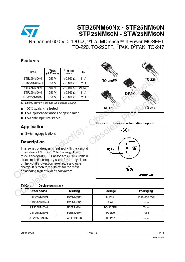
STB25NM60Nx - STF25NM60N STP25NM60N - STW25NM60N N-channel 600 V, 0.130 Ω , 21 A, MDmesh™ II Power MOSFET TO-220, TO-220FP, I2PAK, D2PAK, TO-247 Features Type VDSS (@Tjmax) RDS(on) max ID STB25NM60N t(s)STB25NM60N-1 cSTF25NM60N uSTP25NM60N rod )STW25NM60N 650 V 650 V 650 V 650 V 650 V < 0.160 Ω < 0.160 Ω < 0.160 Ω < 0.160 Ω < 0.160 Ω 21 A 21 A 21 A(1) 21 A 21 A P t(s1. Limited only by maximum temperature allowed te c■ 100% avalanche tested le du■ Low input capacitance and gate charge so ro■ Low gate input resistance - Ob te PApplication ) le■ Switching applications ct(s bsoDescription du - OThis series of devices is realized with the second ro )generation of MDmesh™ technology.