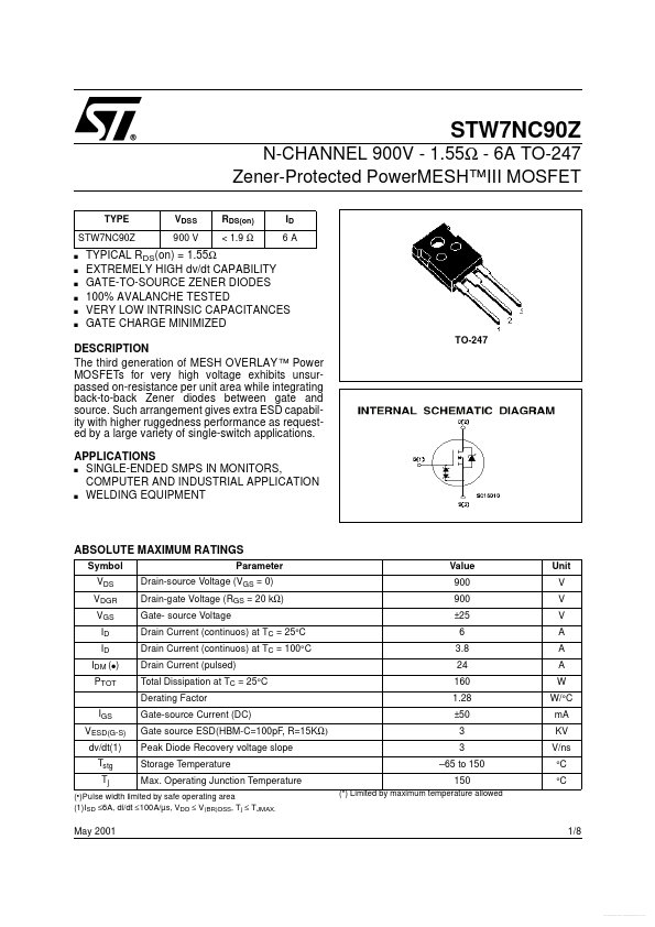
Datasheet4U Logo Datasheet4U.com

W7NC90Z Datasheet STW7NC90Z

Manufacturer: STMicroelectronics

Overview: N-CHANNEL 900V - 1.55Ω - 6A TO-247 Zener-Protected PowerMESH™III MOSFET TYPE STW7NC90Z s s s s s s STW7NC90Z VDSS 900 V RDS(on) < 1.9 Ω ID 6A TYPICAL RDS(on) = 1.

General Description

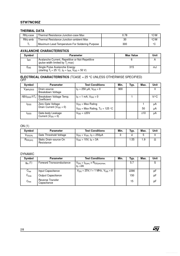
The third generation of MESH OVERLAY ™ Power MOSFETs for very high voltage exhibits unsurpassed on-resistance per unit area while integrating back-to-back Zener diodes between gate and source.

Such arrangement gives extra ESD capability with higher ruggedness performance as requested by a large variety of single-switch applications.

APPLICATIONS s SINGLE-ENDED SMPS IN MONITORS, COMPUTER AND INDUSTRIAL APPLICATION s WELDING EQUIPMENT ABSOLUTE MAXIMUM RATINGS Symbol VDS VDGR VGS ID ID IDM (q ) PTOT IGS VESD(G-S) dv/dt(1) Tstg Tj Parameter Drain-source Voltage (VGS = 0) Drain-gate Voltage (RGS = 20 kΩ) Gate- source Voltage Drain Current (continuos) at TC = 25°C Drain Current (continuos) at TC = 100°C Drain Current (pulsed) Total Dissipation at TC = 25°C Derating Factor Gate-source Current (DC) Gate source ESD(HBM-C=100pF, R=15KΩ) Peak Diode Recovery voltage slope Storage Temperature Max.

Key Features

  • OF GATE-TO-SOURCE ZENER DIODES The built-in back-to-back Zener diodes have specifically been designed to enhance not only the device’s ESD capability, but also to make them safely absorb possible voltage transients that may occasionally be applied from gate to souce. In this respect the 25V Zener voltage is appropiate to achieve an efficient and cost-effective intervention to protect the device’s integrity. These integrated Zener diodes thus avoid the usage of external components. 3/8 Free Dat.