SPC4533W Overview
The SPC4533W is the N- and P-Channel enhancement mode power field effect transistors are produced using high cell density, DMOS trench technology. This high density process is especially tailored to minimize on-state resistance and provide superior switching performance. These devices are particularly suited for low voltage applications such as notebook puter power management and other battery powered circuits where...
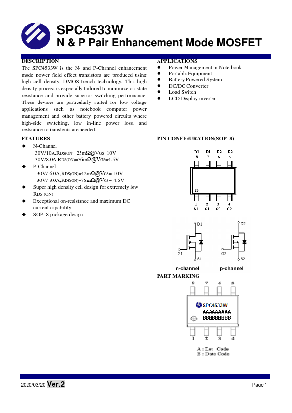
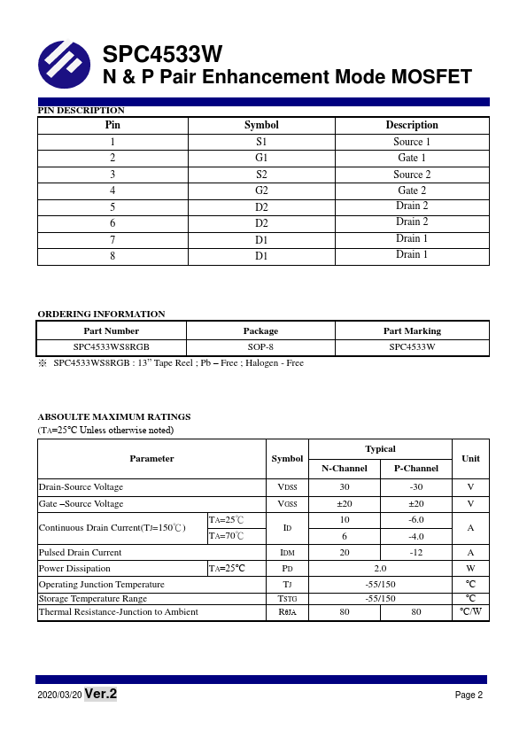
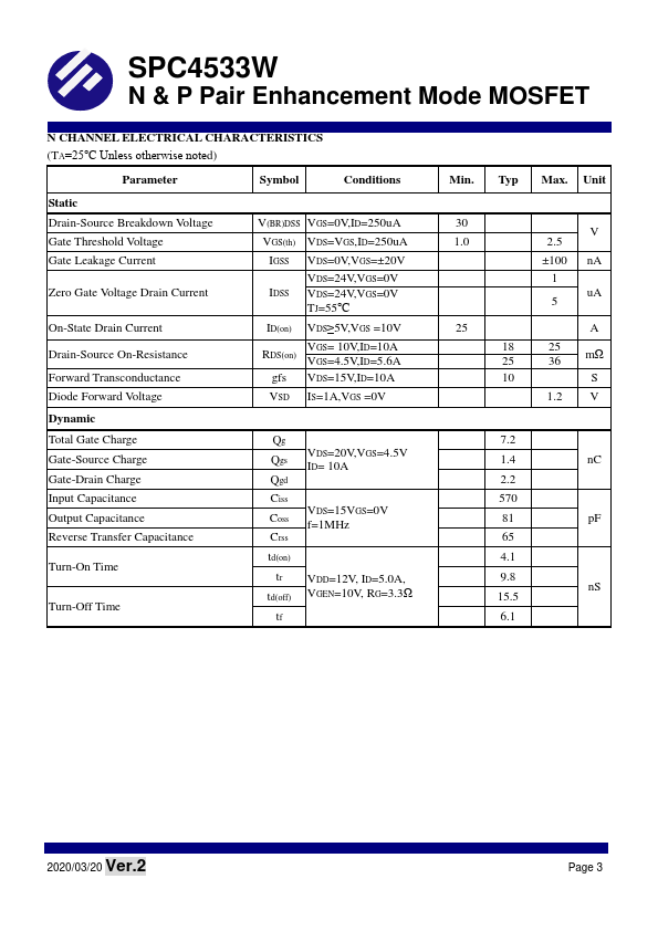
SPC4533W Key Features
- N-Channel
- P-Channel -30V/-6.0A,RDS(ON)=42mΩ@VGS=-10V -30V/-3.0A,RDS(ON)=78mΩ@VGS=-4.5V
- Super high density cell design for extremely low RDS (ON)
- Exceptional on-resistance and maximum DC current capability
- SOP-8 package design
SPC4533W Applications
- Power Management in Note book