N-Channel Enhancement Mode Field Effect Transistor
Full PDF Text Transcription (Reference)
The following content is an automatically extracted verbatim text
from the original manufacturer datasheet and is provided for reference purposes only.
View original datasheet text
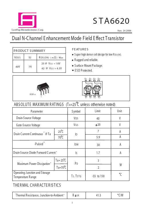
S T A6620
S amHop Microelectronics C orp. Nov. 24 2006
Dual N-C hannel E nhancement Mode Field E ffect Transistor
P R ODUC T S UMMAR Y
V DS S
40V
F E AT UR E S S uper high dense cell design for low R DS (ON ).
ID
7A
R DS (ON) ( m Ω ) Max
25 @ V G S = 10V 42 @ V G S = 4.5V
R ugged and reliable. S urface Mount P ackage. E S D P rotected.
D1
8
D1
7
D2
6
D2
5
P DIP -8 1
1
2
3
4
S1
G1 S 2
G2
ABS OLUTE MAXIMUM R ATINGS (T A=25 C unless otherwise noted)
P arameter Drain-S ource Voltage Gate-S ource Voltage Drain C urrent-C ontinuous @ Ta -P ulsed
b a
S ymbol V DS V GS 25 C 70 C IDM IS PD ID
Limit 40 20 7 5.9 30 1.