Datasheet4U Logo Datasheet4U.com

K4H560838D-TCB3 Datasheet - Samsung Semiconductor

256Mb D-die DDR Sdram

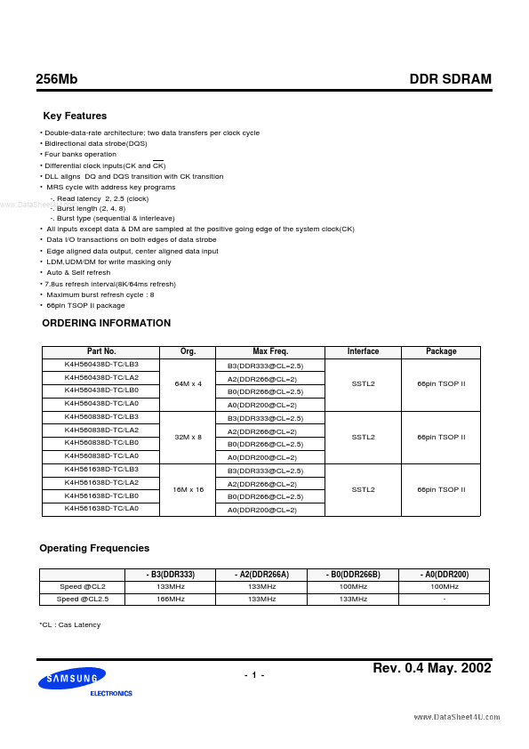
K4H560838D-TCB3 Features

* Double-data-rate architecture; two data transfers per clock cycle

* Bidirectional data strobe(DQS)

* Four banks operation

* Differential clock inputs(CK and CK)

* DLL aligns DQ and DQS transition with CK transition

* MRS cycle with address key progra

K4H560838D-TCB3 General Description

SYMBOL CK, CK DDR SDRAM TYPE Input DESCRIPTION Clock : CK and CK are differential clock inputs. All address and control input signals are sampled on the positive edge of CK and negative edge of CK. Output (read) data is referenced to both edges of CK. Internal clock signals are derived from CK/CK.

K4H560838D-TCB3 Datasheet (205.14 KB)

Preview of K4H560838D-TCB3 PDF

Datasheet Details

Part number:

K4H560838D-TCB3

Manufacturer:

Samsung Semiconductor

File Size:

205.14 KB

Description:

256mb d-die ddr sdram.

📁 Related Datasheet

K4H560838D-TCB0 128Mb DDR SDRAM (Samsung)

K4H560838D-TCA0 128Mb DDR SDRAM (Samsung)

K4H560838D-TCA2 128Mb DDR SDRAM (Samsung)

K4H560838D-TLA0 128Mb DDR SDRAM (Samsung)

K4H560838D-TLA2 128Mb DDR SDRAM (Samsung)

K4H560838D-TLB0 128Mb DDR SDRAM (Samsung)

K4H560838A-TCA0 128Mb DDR SDRAM (Samsung)

K4H560838A-TCA2 128Mb DDR SDRAM (Samsung)

K4H560838A-TCB0 128Mb DDR SDRAM (Samsung)

K4H560838A-TLA0 128Mb DDR SDRAM (Samsung)

TAGS

K4H560838D-TCB3 256Mb D-die DDR Sdram Samsung Semiconductor

Image Gallery

K4H560838D-TCB3 Datasheet Preview Page 2 K4H560838D-TCB3 Datasheet Preview Page 3

K4H560838D-TCB3 Distributor