K7B321825M Description
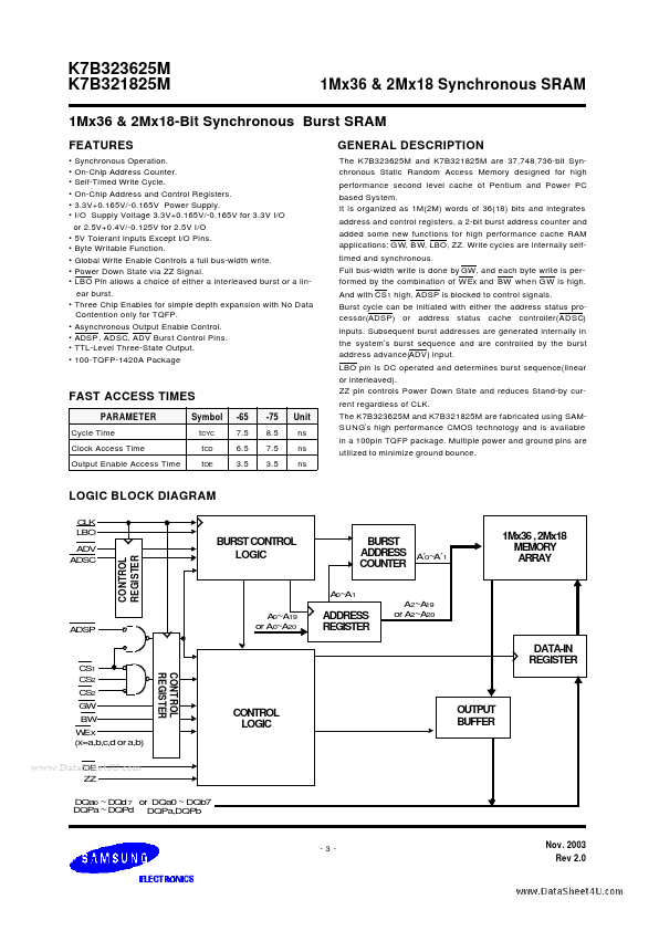
The K7B323625M and K7B321825M are 37,748,736-bit Synchronous Static Random Access Memory designed for high performance second level cache of Pentium and Power PC based System. It is organized as 1M(2M) words of 36(18) bits and integrates address and control registers, a 2-bit burst addr.
K7B321825M Key Features
- Synchronous Operation
- On-Chip Address Counter
- Self-Timed Write Cycle
- On-Chip Address and Control Registers
- 3.3V+0.165V/-0.165V Power Supply
- 5V Tolerant Inputs Except I/O Pins
- Byte Writable Function
- Global Write Enable Controls a full bus-width write
- Power Down State via ZZ Signal
- LBO Pin allows a choice of either a interleaved burst or a linear burst