Datasheet4U Logo Datasheet4U.com

K7B323625M Datasheet 1Mx36 & 2Mx18 Synchronous SRAM

Manufacturer: Samsung Semiconductor

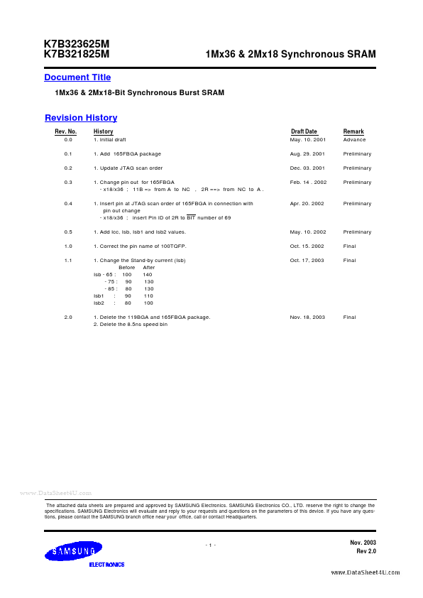
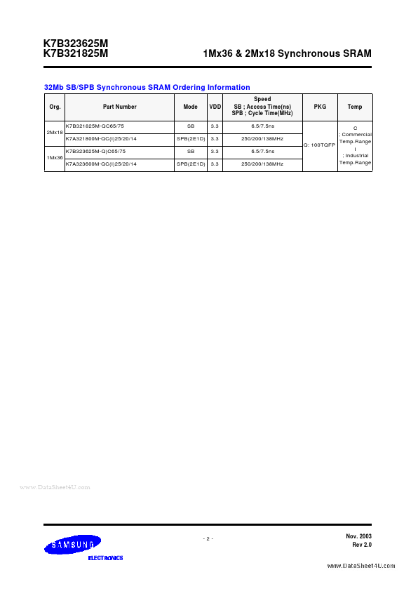
Overview: K7B323625M K7B321825M Document Title 1Mx36 & 2Mx18 Synchronous SRAM 1Mx36 & 2Mx18-Bit Synchronous Burst SRAM Revision History Rev. No. 0.0 0.1 0.2 0.3 History 1. Initial draft 1. Add 165FBGA package 1. Update JTAG scan order 1. Change pin out for 165FBGA - x18/x36 ; 11B => from A to NC , 2R ==> from NC to A . 1. Insert pin at JTAG scan order of 165FBGA in connection with pin out change - x18/x36 ; insert Pin ID of 2R to BIT number of 69 1. Add Icc, Isb, Isb1 and Isb2 values. 1. Correct the pin name of 100TQFP. 1. Change the Stand-by current (Isb) Before After Isb - 65 : 100 140 - 75 : 90 130 - 85 : 80 130 Isb1 : 90 110 Isb2 : 80 100 1. Delete the 119BGA and 165FBGA package. 2. Delete the 8.5ns speed bin Draft Date May. 10. 2001 Aug. 29. 2001 Dec. 03. 2001 Feb. 14 . 2002 Remark Advance Preliminary Preliminary Preliminary 0.4 Apr. 20. 2002 Preliminary 0.5 1.0 1.1 May. 10. 2002 Oct. 15. 2002 Oct. 17, 2003 Preliminary Final Final 2.0 Nov. 18, 2003 Final www.DataSheet4U.com The attached data sheets are prepared and approved by SAMSUNG Electronics. SAMSUNG Electronics CO., LTD. reserve the right to change the specifications. SAMSUNG Electronics will evaluate and reply to your requests and questions on the parameters of this device. If you have any questions, please contact the SAMSUNG branch office near your office, call or contact Headquarters. -1- Nov. 2003 Rev 2.0 K7B323625M K7B321825M 1Mx36 & 2Mx18 Synchronous SRAM 32Mb SB/SPB Synchronous SRAM Ordering Information Org. Part Number Mode VDD Speed SB ; Access Time(ns) SPB ; Cycle Time(MHz) 6.5/7.5ns 250/200/138MHz 6.5/7.5ns 250/200/138MHz PKG Temp K7B321825M-QC65/75 2Mx18 K7A321800M-QC(I)25/20/14 K7B323625M-Q)C65/75 1Mx36 K7A323600M-QC(I)25/20/14 SB SPB(2E1D) SB SPB(2E1D) 3.3 3.3 3.3 3.3 C ; Commercial Temp.Range Q: 100TQFP I ; Industrial Temp.Range www.DataSheet4U.com -2- Nov. 2003 Rev 2.

Download the K7B323625M datasheet PDF. This datasheet also includes the K7B321825M variant, as both parts are published together in a single manufacturer document.

Key Features

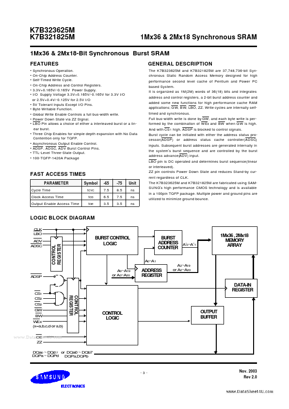
  • Synchronous Operation.
  • On-Chip Address Counter.
  • Self-Timed Write Cycle.
  • On-Chip Address and Control Registers.
  • 3.3V+0.165V/-0.165V Power Supply.
  • I/O Supply Voltage 3.3V+0.165V/-0.165V for 3.3V I/O or 2.5V+0.4V/-0.125V for 2.5V I/O.
  • 5V Tolerant Inputs Except I/O Pins.
  • Byte Writable Function.
  • Global Write Enable Controls a full bus-width write.
  • Power Down State via ZZ Signal.
  • LBO Pin allows.

K7B323625M Distributor & Price

Compare K7B323625M distributor prices and check real-time stock availability from major suppliers. Prices and inventory may vary by region and order quantity.