Datasheet4U Logo Datasheet4U.com

K7K1618U2C Datasheet 512Kx36 & 1Mx18 DDRII CIO b2 SRAM

Manufacturer: Samsung Semiconductor

Overview: K7K1636U2C K7K1618U2C 512Kx36 & 1Mx18 DDRII+ CIO b2 SRAM 18Mb DDRII+ SRAM Specification 165 FBGA with Pb & Pb-Free (RoHS compliant) INFORMATION IN THIS DOCUMENT IS PROVIDED IN RELATION TO SAMSUNG PRODUCTS, AND IS SUBJECT TO CHANGE WITHOUT NOTICE. NOTHING IN THIS DOCUMENT SHALL BE CONSTRUED AS GRANTING ANY LICENSE, EXPRESS OR IMPLIED, BY ESTOPPEL OR OTHERWISE, TO ANY INTELLECTUAL PROPERTY RIGHTS IN SAMSUNG PRODUCTS OR TECHNOLOGY. ALL INFORMATION IN THIS DOCUMENT IS PROVIDED ON AS "AS IS" BASIS WITHOUT GUARANTEE OR WARRANTY OF ANY KIND. 1. For updates or additional information about Samsung products, contact your nearest Samsung office. 2. Samsung products are not intended for use in life support, critical care, medical, safety equipment, or similar applications where Product failure couldresult in loss of life or personal or physical harm, or any military or defense application, or any governmental procurement to which special terms or provisions may apply. www.DataSheet4U.com * Samsung Electronics reserves the right to change products or specification without notice. -1- Rev. 1.1 August 2010 K7K1636U2C K7K1618U2C Document Title 512Kx36 & 1Mx18 DDRII+ CIO b2 SRAM 512Kx36-bit, 1Mx18-bit DDRTM II+ CIO b2 SRAM Revision History Rev. No. 1.0 1.1 History 1. First release 1. Corrected the Timing Diagram of CL2.5 on page.15 2. Corrected Package Dimensions on page.19 Draft Date Aug. 28, 2008 Aug. 10, 2010 Remark Final Final www.DataSheet4U.com The attached data sheets are prepared and approved by SAMSUNG Electronics. SAMSUNG Electronics CO., LTD. reserve the right to change the specifications. SAMSUNG Electronics will evaluate and reply to your requests and questions on the parameters of this device. If you have any questions, please contact the SAMSUNG branch office near your office, call or contact Headquarters. -2- Rev. 1.

Key Features

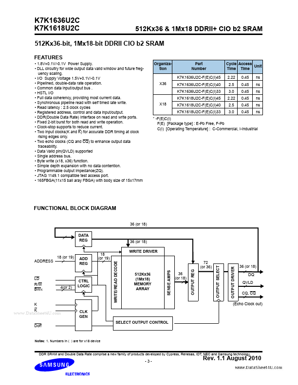
  • 1.8V+0.1V/-0.1V Power Supply.
  • DLL circuitry for wide output data valid window and future freguency scaling.
  • I/O Supply Voltage 1.5V+0.1V/-0.1V.
  • Pipelined, double-data rate operation.
  • Common data input/output bus.
  • HSTL I/O.
  • Full data coherency, providing most current data.
  • Synchronous pipeline read with self timed late write.
  • Read latency : 2.5 clock cycles.
  • Registered address, control and data input.