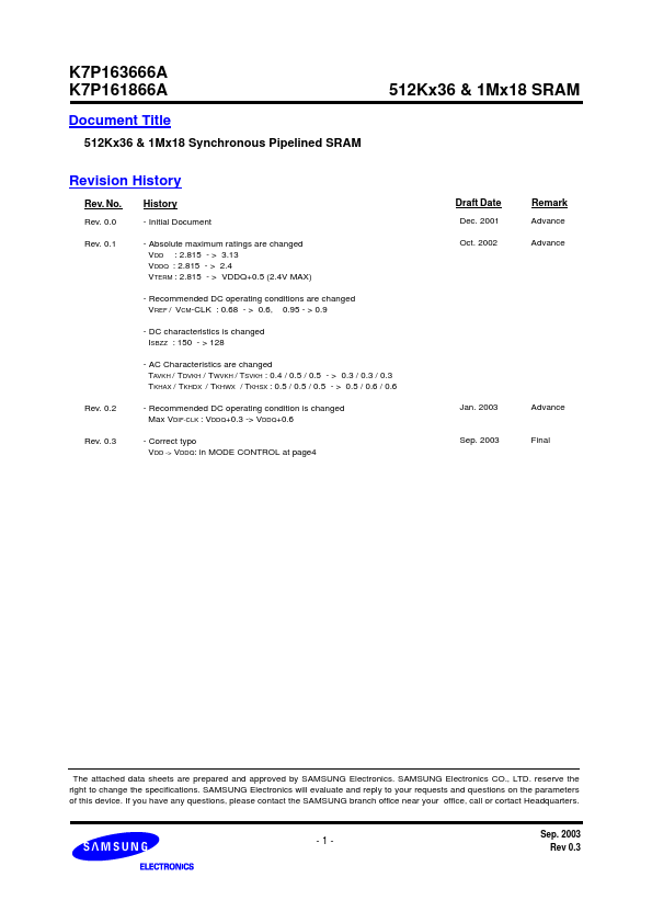
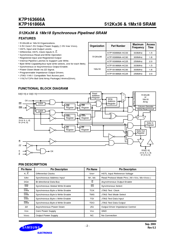
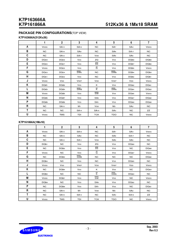
Datasheet4U Logo Datasheet4U.com

K7P161866A - (K7P161866A / K7P163866A) 512Kx36 AND 1Mx18 Synchronous Pipelined SRAM

Description

Pin Name K, K SAn DQn SW SWa SWb SWc SWd ZZ VDD VDDQ Pin Description Differential Clocks Synchronous Address Input Bi-directional Data Bus Synchronous Global Write Enable Synchronous Byte a Write Enable Synchronous Byte b Write Enable Synchronous Byte c Write Enable Synchronous Byte d Write Enable A

Features

  • 512Kx36 or 1Mx18 Organizations.
  • 2.5V Core/1.5V Output Power Supply (1.9V max VDDQ).
  • HSTL Input and Output Levels.
  • Differential, HSTL Clock Inputs K, K.
  • Synchronous Read and Write Operation.
  • Registered Input and Registered Output.
  • Internal Pipeline Latches to Support Late Write.
  • Byte Write Capability(four byte write selects, one for each 9bits).
  • Synchronous or Asynchronous Output Enable.
  • Power Down Mo.

📥 Download Datasheet

Full PDF Text Transcription (Reference)

The following content is an automatically extracted verbatim text from the original manufacturer datasheet and is provided for reference purposes only.

View original datasheet text
www.DataSheet4U.com K7P163666A K7P161866A Document Title 512Kx36 & 1Mx18 Synchronous Pipelined SRAM 512Kx36 & 1Mx18 SRAM Revision History Rev. No. Rev. 0.0 Rev. 0.1 History - Initial Document - Absolute maximum ratings are changed VDD : 2.815 - > 3.13 VDDQ : 2.815 - > 2.4 VTERM : 2.815 - > VDDQ+0.5 (2.4V MAX) - Recommended DC operating conditions are changed VREF / VCM-CLK : 0.68 - > 0.6, 0.95 - > 0.9 - DC characteristics is changed ISBZZ : 150 - > 128 - AC Characteristics are changed TAVKH / TDVKH / TWVKH / TSVKH : 0.4 / 0.5 / 0.5 - > 0.3 / 0.3 / 0.3 TKHAX / TKHDX / TKHWX / TKHSX : 0.5 / 0.5 / 0.5 - > 0.5 / 0.6 / 0.6 Draft Date Dec. 2001 Oct. 2002 Remark Advance Advance Rev. 0.2 - Recommended DC operating condition is changed Max VDIF-CLK : VDDQ+0.3 -> VDDQ+0.
Published: |