K7Q163662B Description
Final spec release Draft Date Jan. 18, 2004 Remark Advance Final The attached data sheets are prepared and approved by SAMSUNG Electronics. SAMSUNG Electronics CO., LTD.
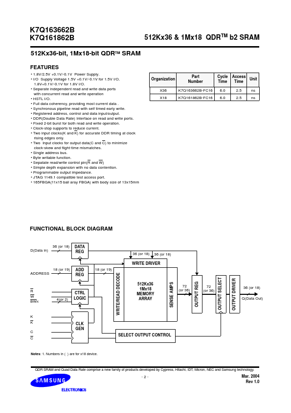
K7Q163662B Key Features
- 1.8V/2.5V +0.1V/-0.1V Power Supply
- Separate independent read and write data ports with concurrent read and write operation
- HSTL I/O
- Full data coherency, providing most current data
- Synchronous pipeline read with self timed early write
- Registered address, control and data input/output
- DDR(Double Data Rate) Interface on read and write ports
- Fixed 2-bit burst for both read and write operation
- Clock-stop supports to reduce current
- Two input clocks(K and K) for accurate DDR timing at clock rising edges only