SIM6800M/MV Series
Contents
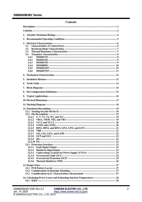
Description ------------------------------------------------------------------------------------------------------ 1
Contents --------------------------------------------------------------------------------------------------------- 2
1. Absolute Maximum Ratings----------------------------------------------------------------------------- 4
2. Recommended Operating Conditions ----------------------------------------------------------------- 5
3. Electrical Characteristics -------------------------------------------------------------------------------- 6
3.1 Characteristics of Control Parts------------------------------------------------------------------ 6
3.2 Bootstrap Diode Characteristics ----------------------------------------------------------------- 7
3.3 Thermal Resistance Characteristics ------------------------------------------------------------- 7
3.4 Transistor Characteristics ------------------------------------------------------------------------- 8
3.4.1 SIM6811M -------------------------------------------------------------------------------------- 8
3.4.2 SIM6812M -------------------------------------------------------------------------------------- 9
3.4.3 SIM6813M -------------------------------------------------------------------------------------- 9
3.4.4 SIM6880M ------------------------------------------------------------------------------------ 10
3.4.5 SIM6822MV---------------------------------------------------------------------------------- 10
3.4.6 SIM6827MV---------------------------------------------------------------------------------- 11
4. Mechanical Characteristics --------------------------------------------------------------------------- 12
5. Insulation Distance-------------------------------------------------------------------------------------- 12
6. Truth Table----------------------------------------------------------------------------------------------- 13
7. Block Diagrams ------------------------------------------------------------------------------------------ 14
8. Pin Configuration Definitions------------------------------------------------------------------------- 15
9. Typical Applications ------------------------------------------------------------------------------------ 16
10. Physical Dimensions ------------------------------------------------------------------------------------ 17
11. Marking Diagram --------------------------------------------------------------------------------------- 18
12. Functional Descriptions -------------------------------------------------------------------------------- 19
12.1 Turning On and Off the IC---------------------------------------------------------------------- 19
12.2 Pin Descriptions ----------------------------------------------------------------------------------- 19
12.2.1 U, V, V1, V2, W1, and W2 ----------------------------------------------------------------- 19
12.2.2 VB1A, VB1B, VB2, and VB3-------------------------------------------------------------- 19
12.2.3 VCC1 and VCC2 ---------------------------------------------------------------------------- 20
12.2.4 COM1 and COM2--------------------------------------------------------------------------- 20
12.2.5 HIN1, HIN2, and HIN3; LIN1, LIN2, and LIN3 -------------------------------------- 21
12.2.6 VBB -------------------------------------------------------------------------------------------- 21
12.2.7 LS1, LS2, LS3A, and LS3B---------------------------------------------------------------- 22
12.2.8 OCP and OCL ------------------------------------------------------------------------------- 22
12.2.9 SD----------------------------------------------------------------------------------------------- 22
12.2.10 FO ---------------------------------------------------------------------------------------------- 22
12.3 Protection Functions------------------------------------------------------------------------------ 23
12.3.1 Fault Signal Output ------------------------------------------------------------------------- 23
12.3.2 Shutdown Signal Input --------------------------------------------------------------------- 23
12.3.3 Undervoltage Lockout for Power Supply (UVLO) ----------------------------------- 23
12.3.4 Overcurrent Limit (OCL) ----------------------------------------------------------------- 24
12.3.5 Overcurrent Protection (OCP) ----------------------------------------------------------- 25
12.3.6 Thermal Shutdown (TSD) ----------------------------------------------------------------- 26
13. Design Notes ---------------------------------------------------------------------------------------------- 27
13.1 PCB Pattern Layout ------------------------------------------------------------------------------ 27
13.2 Considerations in Heatsink Mounting -------------------------------------------------------- 27
13.3 Considerations in IC Characteristics Measurement --------------------------------------- 27
14. Calculating Power Losses and Estimating Junction Temperatures --------------------------- 28
14.1 IGBT ------------------------------------------------------------------------------------------------- 28
SIM6800M/MV-DSE Rev.2.2
SANKEN ELECTRIC CO., LTD
Jan. 15, 2020
https://www.sanken-ele.co.jp/en
© SANKEN ELECTRIC CO., LTD. 2014
2