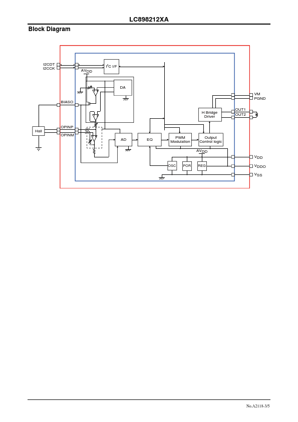
I INPUT O OUTPUT B BIDIRECTION
LC898212XA
TYPE P Power supply, GND NC NOT CONNECT
I2C interface I2CCK I2CDT
B I2C Clock pin B I2C Data pin
D/A interface BIASO
O D/A output (Hall bias input)
Op-Amp interface OPINP OPINM
I I
Op-Amp input Op-Amp input
Driver interface OUT1
OUT2
O Actuator out
Key Features
Built-in equalizer circuit using digital operation AF control equalize circuit Any coefficient can be specified by I2C I/F.
I2C Interface.
Built-in A/D converter
Maximum 10-bit Input 2 channel.
Full PDF Text Transcription for LC898212XA (Reference)
Note: Below is a high-fidelity text extraction (approx. 800 characters) for
LC898212XA. For precise diagrams, and layout, please refer to the original PDF.
Ordering number : ENA2118A LC898212XA CMOS LSI AF Control LSI Overview The AF control device, LC898212XA (LC898212XA-MH), provides an ideal way to implement the reduced p...
View more extracted text
12XA (LC898212XA-MH), provides an ideal way to implement the reduced power consumption and the improved autofocus precision and speed (reduced convergence time) required in high-pixelcount camera modules for use in smartphones. The LC898212XA integrates on a single chip an equalizer circuit employing digital calculation, and it can be combined with position sensors to build a closed-loop actuator control system. Since closed-loop control provides better ability to maintain the control object than conventional open-loop systems and is not affected by position differences, the LC898212XA is ideal for use in AF systems used i
 LC898212XA Datasheet