Part number:
LC8991
Manufacturer:
Sanyo
File Size:
39.24 KB
Description:
Ntsc ccd 1h delay line.
LC8991 Features
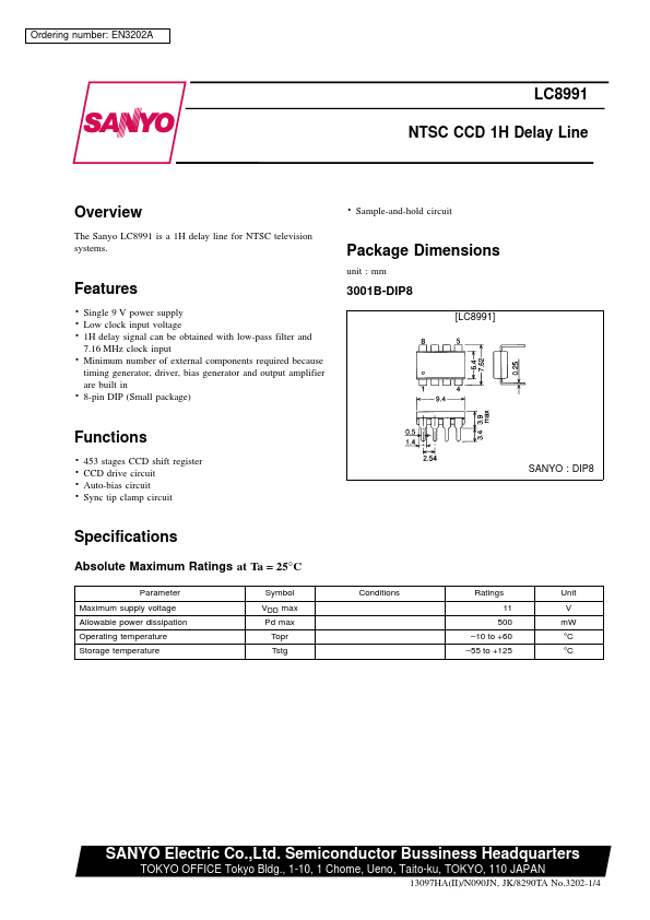
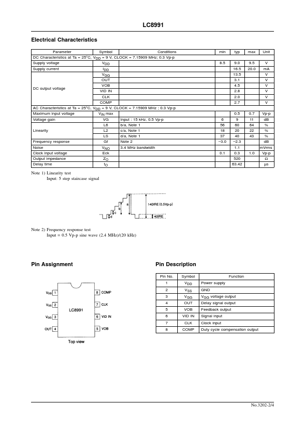
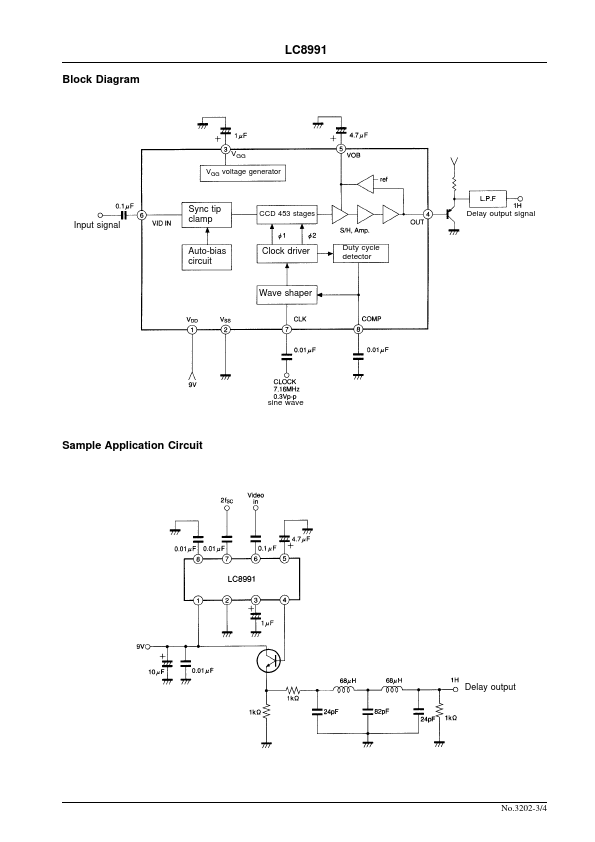
* 3001B-DIP8 [LC8991] . Single 9 V power supply . Low clock input voltage . 1H delay signal can be obtained with low-pass filter and MHz clock input . 7.16 Minimum number of external components required because . timing generator, driver, bias generator and output amplifier are built in 8-pin DIP (S
Datasheet Details
LC8991
Sanyo
39.24 KB
Ntsc ccd 1h delay line.
📁 Related Datasheet
LC8991 Distributor