2N6500 Overview
Key Specifications
Description
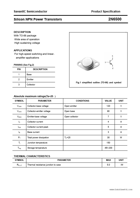
With TO-66 package - Wide area of operation - High sustaining voltage APPLICATIONS - For high-speed switching and linearamplifier applications PINNING (See Fig.2) PIN 1 2 3 Base Emitter Collector Fig.1 simplified outline (TO-66) and symbol DESCRIPTION SYMBOL VCBO VCEO VEBO IC ICM IB PT Tj Tstg PARAMETER Collector-base voltage Collector-emitter voltage Emitter-base voltage Collector current Collector current-peak Base current Total power dissipation Junction temperature Storage temperature TC=25 CONDITIONS Open emitter Open base Open collector VALUE 120 90 7 4 5 3 35 150 -65~200 UNIT V V V A A A W SYMBOL Rth j-C PARAMETER SavantIC Semiconductor Product Specification Silicon NPN Power Transistors CHARACTERISTICS Tj=25 unless otherwise specified PARAMETER CONDITIONS MIN TYP. 2N6500 SYMBOL MAX UNIT VCEO(SUS) Collector-emitter sustaining voltage IC=0.2 A ; IB=0 90 V VCEsat Collector-emitter saturation voltage IC=3A; IB=0.3A 1.5 V VBEsat Base -emitter saturation voltage IC=3A; IB=0.3A VCE=110V;VBE(off)=-1.5V TC=150 VCE=70V; IB=0 2.5 5.0 10 5.0 V ICEV Collector cut-off current mA ICEO Collector cut-off current mA IEBO Emitter cut-off current VEB=7V; IC=0 25 mA hFE DC current gain IC=3A ; VCE=2V 15 60 COB Output capacitance IE=0 ; VCB=10V;f=1MHz 175 pF 2 SavantIC Semiconductor Product Specification Silicon NPN Power Transistors PACKAGE OUTLINE 2N6500 Fig.2 Outline dimensions 3.