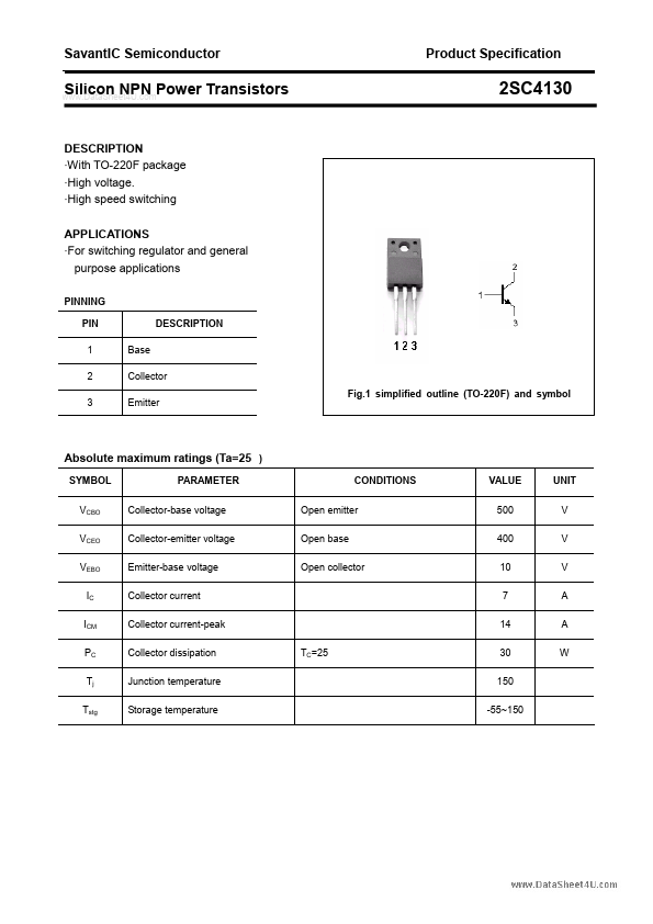
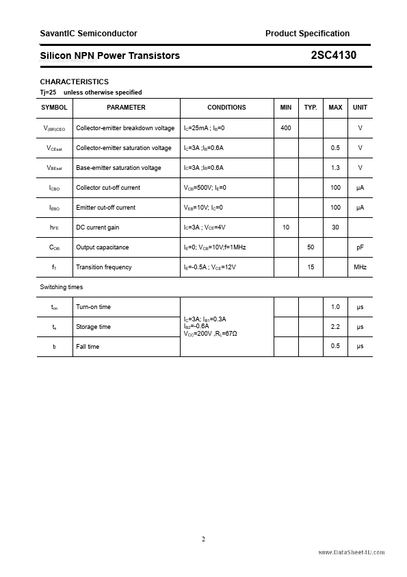
High speed switching APPLICATIONS
For switching regulator and general purpose applications
PINNING PIN 1 2 3 Base Collector Emitter Fig.1 simplified outline (TO-220F) and symbol DESCRIPTION
Absolute maximum ratings (Ta=25 )
SYMBOL VCBO VCEO VEB
Full PDF Text Transcription for 2SC4130 (Reference)
Note: Below is a high-fidelity text extraction (approx. 800 characters) for
2SC4130. For precise diagrams, and layout, please refer to the original PDF.
30 DESCRIPTION ·With TO-220F package ·High voltage. ·High speed switching APPLICATIONS ·For switching regulator and general purpose applications PINNING PIN 1 2 3 Base Collector Emitter Fig.1 simplified outline (TO-220F) and symbol DESCRIPTION Absolute maximum ratings (Ta=25 ) SYMBOL VCBO VCEO VEBO IC ICM PC Tj Tstg PARAMETER Collector-base voltage Collector-emitter voltage Emitter-base voltage Collector current Collector current-peak Collector dissipation Junction temperature Storage temperature TC=25 CONDITIONS Open emitter Open base Open collector VALUE 500 400 10 7 14 30 150 -55~150 UNIT V V V A A W SavantIC Semiconduc